






| MODELL P/N | SERIE | ANZAHL DER LABORE/KLINIKEN | GESCHWINDIGKEITSSTUFE | ANZAHL DER LOGIKELEMENTE / ZELLEN | RAM-BITS INSGESAMT | ANZAHL DER E/A | SPANNUNG - VERSORGUNG | BEFESTIGUNGSTYP | BETRIEBSTEMPERATUR | VERPACKUNG / KASSE | LIEFERANT GERÄTEPAKET |
|---|---|---|---|---|---|---|---|---|---|---|---|
| XCVU190-1FLGB2104I | Virtex® UltraScale (XCVU190) | 134,28 | -1,00 | 2.349.900 LE | 150.937.600 Bits (150,9 Mbit) | 702 | ~0,922-0,979 V (aufgeführte Bereiche) | Oberflächenmontage | -40°C ~ +100°C (TJ) | FBGA-2104 / FCBGA-2104 | 2104-FCBGA |
XCVU190-1FLGB2104I
Hersteller: Xilinx
Logische Zellen: 2,100,000
Logische Schnitte: 328,000
Eingebettetes RAM (eRAM): 75.960 Kb (2.110 × 36Kb Block RAM)
Maximale Benutzer-E/A: 850
Paket: FLGB2104 (Flip-Chip BGA)
Geschwindigkeitsstufe: -1
Betriebstemperatur: Industriell (-40°C bis +100°C)
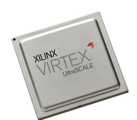
Spezifikationen
Definition der Artikelnummer
This industrial temperature FPGA is part of Xilinx Virtex UltraScale series, manufactured with 20nm FinFET process technology. It features moderate overall logic capacity, rich arithmetic and memory resources together with high-speed serial interfaces, tailored for power-sensitive rugged embedded devices, aerospace payload systems and industrial high-speed signal processing equipment that require stable operation within the full industrial temperature range.
- XCVU190: Mid-high density device of Virtex UltraScale family, equipped with complete high-speed interconnection architecture
- -1: Speed Grade 1, low-power optimized timing grade. It focuses on power consumption reduction and thermal stability rather than maximum operating frequency, ideal for devices with limited heat dissipation space and long-duration continuous running demands
- FLGB2104: 2104-ball flip-chip FCBGA compact package. The reduced package size enables hardware miniaturization while retaining adequate pins for transceiver layout, parallel signal access and peripheral circuit expansion
- I: Industrial temperature specification, junction temperature operating range: -40°C ~ +100°C
Details zu den On-Chip-Hardware-Ressourcen
1. Programmierbare Logikressourcen
- Total Logic Cells: 1938720
- Configurable CLB Slices: 110640
- Total Flip-Flops: 2212800
- Total LUTs: 1106400
2. Arithmetic and Embedded Memory Resources
- DSP48E2 arithmetic blocks: 1728 units, capable of fixed-point and floating-point calculations, large-scale FFT operations, radar signal modulation and demodulation, encryption algorithm acceleration and medium-sized matrix computing
- Total Block RAM: 53.2 Mb, applied to image frame buffering, deep FIFO data caching, waveform recording and algorithm parameter storage tables
- Distributed RAM: 14.6 Mb, used for on-chip small temporary cache and lightweight asynchronous data buffering
3. Clock Management System
- 16 MMCM clock management tiles
- 16 PLL phase-locked loops
Multiple independent clock domains can be configured freely, supporting clock phase adjustment, transmission delay compensation and high-frequency jitter suppression, which meets strict timing synchronization requirements of complex large digital systems
4. Serielle Hochgeschwindigkeits-Transceiver
- 32 GTH differential high-speed transceivers
Each lane supports a maximum transmission rate of 32.75 Gbps, compatible with PCIe Gen4, 100G Ethernet, Aurora, JESD204B and other mainstream high-speed serial protocols. Built-in hard network IP cores simplify the development of high-bandwidth communication interfaces
5. I/O Resources and System Monitoring Module
- Configurable user I/O pins: 936
Multiple I/O voltage domains from 1.2V to 3.3V are available, fully compatible with LVCMOS, LVDS, HSTL, SSTL and all commonly used single-ended and differential signal standards
The built-in system monitoring module collects real-time data of chip junction temperature, internal power supply voltages and external analog input signals continuously
Technische Daten zum Netzteil
Core working voltage ranges from 0.85V to 0.9V. Logic area, block RAM, DSP arrays and serial transceivers adopt independent power domains, allowing partial module power shutdown to lower total power consumption flexibly
Typical total power consumption ranges from 20W to 56W. For stable full-load operation under the upper industrial temperature limit, forced air cooling is required
Anforderungen an die Verpackung und die SMT
- Package type: 2104-pin FCBGA flip-chip ball grid array
- Moisture Sensitivity Level: MSL4. Reflow soldering must be completed within 72 hours after the vacuum package is opened
- Lead-free packaging design, compliant with RoHS environmental regulations
- Chips are stored and transported in anti-static trays to prevent electrostatic damage during mass PCB assembly
Umgebungsanpassungsfähigkeit und Zuverlässigkeit
The chip can operate stably for a long time under drastic temperature changes, mechanical shock, vibration and strong electromagnetic interference conditions. It supports AES bitstream encryption, partial dynamic reconfiguration, SEU error detection and correction, with enhanced radiation resistance, suitable for aerospace, military portable equipment and field industrial harsh environment deployment
Typische Anwendungsszenarien
- Miniaturized airborne radar signal processing boards, unmanned aerial vehicle payload computing units
- Compact rugged VPX embedded mainboards for defense industry
- Portable high-precision spectrum analyzers and signal generation instruments
- Industrial multi-channel high-speed data acquisition and real-time processing systems
- Medium-scale chip prototype verification platforms with limited installation space
- Vehicular intelligent perception data fusion and gateway processing equipment


