





| MODEL P/N | SERIES | NUMBER OF LABS/CLBS | SPEED GRADE | NUMBER OF LOGIC ELEMENTS / CELLS | TOTAL RAM BITS | NUMBER OF I/O | VOLTAGE – SUPPLY | MOUNTING TYPE | OPERATING TEMPERATURE | PACKAGE / CASE | SUPPLIER DEVICE PACKAGE |
|---|---|---|---|---|---|---|---|---|---|---|---|
| XCKU3P-L1FFVB676I | Kintex® UltraScale+ | 20,34 | 0,00 | 355,950 LE | 31,641,600 bits | 272 | 0.850 V | Surface Mount | -40 °C – +100 °C | FCBGA-676 | 676-FCBGA (27×27) |
XCKU3P-L1FFVB676I
Manufacturer: Xilinx
Logic Cells: 3,780,000
Logic Slices: 590,000
Embedded RAM (eRAM): 81,360 Kb (2,260 × 36Kb Block RAM)
Maximum User I/O: 350
Package: FFVB676 (Flip-Chip BGA)
Speed Grade: -1L
Operating Temperature: Industrial (-40°C to +100°C)
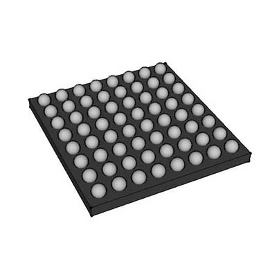
Specifications
Part Number Full Definition
This is AMD Xilinx Kintex UltraScale+ low-power FPGA built on 16nm FinFET process, optimized for ultra-low static power embedded applications.
- XCKU3P: Entry mid-range device of Kintex UltraScale+ series with integrated UltraRAM large-capacity on-chip memory
- L1: Low-power optimized speed grade 1 (LI). Supports dual core voltage operation: 0.85V for standard timing, or 0.72V for maximum power saving with reduced operating frequency; lowest power consumption tier for this chip model
- FFVB676: 676-ball flip-chip FCBGA compact package, die size 27mm × 27mm, ball pitch 1.0mm
- I: Industrial temperature grade, junction temperature operating range: -40°C ~ +100°C
On-Chip Core Hardware Resources
Logic & DSP Arithmetic Units
- Total System Logic Cells: 356,000
- Total LUTs: 163,000
- Total Flip-Flops: 325,000
- DSP48E2 dedicated arithmetic slices: 1368 units
Applied for digital filtering, FFT computation, wireless baseband preprocessing, lightweight image algorithm acceleration and small matrix calculations
Embedded Memory Resources
- Block RAM total capacity: 12.7 Mb
- UltraRAM dedicated large memory: 13.5 Mb (unique advantage of P-series chips, ideal for frame buffer, deep data buffering)
- Distributed RAM (LUT-based): 4.7 Mb for ultra-low latency temporary cache
Clock Management Subsystem
4 Clock Management Tiles (CMT) integrated, each containing MMCM + PLL modules. Realizes clock multiplication/division, arbitrary phase shifting and jitter suppression to satisfy multi-clock domain system timing demands
High-Speed Serial Transceivers & General I/O
- 8-channel GTH high-speed differential transceivers, maximum single lane rate: 16.375 Gbps
Supported protocols: PCIe Gen3, JESD204B/C, 10G Ethernet, Aurora serial transmission
- Available user configurable I/O pins: 280
Includes HR wide-voltage I/O banks and HP high-performance I/O banks; compatible with LVCMOS, LVDS, HSTL, SSTL and mainstream differential signal standards
- Built-in SYSMON system monitor: real-time detection of chip junction temperature, internal power rail voltages and external analog input signals
Power Supply Specifications
- Standard core voltage: 0.85 V
- Low-power mode core voltage: 0.72 V (greatly cuts static & dynamic power consumption, timing performance downgraded to L1 baseline level)
Independent power domains assigned for core logic, UltraRAM, Block RAM, transceivers and I/O banks
Typical total power consumption: 7W ~ 26W; passive heat dissipation is available for compact portable embedded hardware
Packaging & SMT Assembly Requirements
- Package: 676-pin flip-chip FCBGA ball grid array
- Moisture Sensitivity Level: MSL4; all reflow soldering must be finished within 72 hours after vacuum packaging unsealed
- Fully lead-free, RoHS3 & REACH compliant
- Delivered in anti-static trays for automated industrial PCB mass production
Environmental & Reliability Features
Stable continuous operation under wide temperature swings and strong electromagnetic interference industrial environments.
Supports 256-bit AES bitstream encryption for IP protection, SEU single-event upset radiation correction, partial dynamic reconfiguration; tailored for battery-powered portable devices, vehicle electronics and airborne lightweight terminals requiring long runtime and high stability.
Typical Application Scenarios
- Portable software-defined radio, handheld wireless signal transceiving and baseband processing modules
- Battery-powered multi-channel data recorders, vibration monitoring and portable precision measuring instruments
- Miniature airborne short-range radar front-end echo signal acquisition & processing boards
- Vehicle-mounted peripheral control units, in-vehicle low-power video preprocessing terminals
- Compact embedded machine vision inspection equipment for field industrial use
- Low-power PCIe high-speed data acquisition cards and custom industrial SOM core boards


