





| Mfr Part | Manufacturer | FPGA Family | Logic Elements (LEs) | Embedded Memory | DSP / Multipliers | Max I/O Count | Core Voltage | I/O Voltage | Operating Temperature | Package | Process Node | Typical Max Frequency | Target Applications | RoHS |
| 5CEBA2F17C8N | ALTERA | Cyclone® IV E | ~25,000 (family class) | Family dependent | Family dependent | Package dependent | 1.15–1.25 V | Up to 3.3 V | −40 °C to +85 °C | FBGA | 60 nm | ~200 MHz | Industrial logic, communication control | Yes |
5CEBA2F17C8N
Manufacturer: Altera (Intel)
Logic Cells: 25,000 Logic Elements (approx.)
Logic Slices: Adaptive Logic Modules (ALMs)
Embedded RAM (eRAM): 1 Mbit embedded memory
Package: FBGA-256
Operating Temperature: Commercial (0 °C to +85 °C)
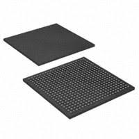
Specifications
5CEBA2F17C8N is an Intel (Altera) Cyclone V E cost-optimized FPGA built on 28nm low-power process, designed for medium-scale digital logic, low-to-mid DSP acceleration and compact embedded control hardware with balanced power consumption and hardware resource density.
👉 It’s not a high-end multi-gigabit transceiver FPGA or ARM integrated SoC FPGA.
👉 It’s a low-power, cost-effective standalone logic FPGA targeting cost-sensitive industrial, communication and educational embedded digital systems.
Key Features of 5CEBA2F17C8N Cyclone V FPGA
Digital hardware and embedded engineers choose 5CEBA2F17C8N for its efficient logic resource, low static power and compact small-form-factor packaging:
- Total 25,000 logic elements (LEs), 9,434 8-input adaptive logic modules (ALMs) for medium-complexity parallel logic design
- Total on-chip memory of 2,002,944 bits, including 1,760 Kbit M10K block RAM + 196 Kbit distributed MLAB RAM for FIFO, cache and frame buffer storage
- 50 built-in 18×18-bit variable-precision DSP multipliers to accelerate filtering, PID control and lightweight signal processing algorithms
- Four independent fractional PLL clock modules supporting internal clock frequency up to 800 MHz for high-speed timing design
- -8 commercial speed grade, optimized timing closure for mainstream medium-frequency operation scenarios
- 256-pin 17×17mm FBGA wirebond package with 128 user-configurable general-purpose I/O pins for peripheral interconnection
- 1.07V–1.13V core supply voltage, supports multi-standard I/O voltages: 1.2V, 1.5V, 1.8V, 2.5V, 3.3V LVTTL/LVCMOS
- Hard DDR3 memory controller IP native integrated, supporting 400MHz DDR3 SDRAM for high-bandwidth data buffering
- Supports full configuration modes: JTAG, Active Serial (AS), Passive Parallel, compatible with EPCS serial flash storage
- Native Nios II soft-core processor support to build custom single-chip embedded SoC without external CPU chips
- Up to 40% lower total power consumption compared to previous Cyclone II/III generation FPGAs, ideal for fanless compact equipment
- Commercial operating temperature range: 0°C to +85°C junction temperature
- RoHS3 compliant lead-free packaging, MSL 3 moisture sensitivity rating for standard SMT mass production
- Stable long-lifecycle component supply for small-batch industrial equipment upgrade and legacy maintenance projects
Typical applications
Mid-size FPGA development boards, university digital electronics teaching platforms
Industrial sensor multi-channel signal acquisition and preprocessing modules
Low-speed wired communication protocol conversion and gateway logic boards
Servo & stepper motor multi-axis motion control systems
Audio/video lightweight real-time signal filtering and image pre-processing
Portable test & measurement instruments and timing generator hardware
Industrial automation PLC auxiliary logic and digital IO expansion boards
LED large screen display driving and high-speed data transmission control units
Medical portable diagnostic equipment digital logic control subsystems
Cost-sensitive consumer industrial IoT edge data processing terminals
LXB Semicon supplies original 5CEBA2F17C8N FPGA


