






| MODELL P/N | SERIE | ANZAHL DER LABORE/KLINIKEN | GESCHWINDIGKEITSSTUFE | ANZAHL DER LOGIKELEMENTE / ZELLEN | RAM-BITS INSGESAMT | ANZAHL DER E/A | SPANNUNG - VERSORGUNG | BEFESTIGUNGSTYP | BETRIEBSTEMPERATUR | VERPACKUNG / KASSE | LIEFERANT GERÄTEPAKET |
|---|---|---|---|---|---|---|---|---|---|---|---|
| XC7Z100-1FFG900C | Zynq-7000 | 26.150,00 | -1,00 | 277,400 | 26200000 | 250 | 1.0 V | Oberflächenmontage | Handelsüblich (0 °C ~ 85 °C) | BGA-900 | 900-FCBGA (31×31 mm) |
XC7Z100-1FFG900C
Hersteller: Xilinx
Logische Zellen: 444,000
Logische Schnitte: 69,000
Eingebettetes RAM (eRAM): 26,280 Kb (730 × 36Kb Block RAM)
Maximale Benutzer-E/A: 300
Paket: FFG900 (Flip-Chip BGA)
Geschwindigkeitsstufe: -1
Betriebstemperatur: Handelsüblich (0°C bis +85°C)
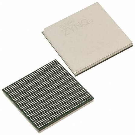
Spezifikationen
Definition der Artikelnummer
This is the highest-speed commercial-grade flagship heterogeneous all-programmable SoC of AMD Xilinx Zynq-7000 family, manufactured on mature 28nm semiconductor process. It combines dual-core ARM Cortex-A9 processing subsystem and maximum-capacity Kintex-7 FPGA programmable logic, specially optimized for ultra-high-frequency complex digital logic, high-throughput signal processing and high-speed data transmission applications running in stable indoor constant-temperature environments.
- XC7Z100: Top flagship model of Zynq-7000 series, equipped with the largest full-set Kintex-7 FPGA resources across the entire product lineup
- -1: Speed Grade 1, premium highest-speed timing tier. It features the shortest signal propagation delay, maximum achievable operating frequency and optimal timing closure performance, exclusively used for demanding ultra-high-speed logic designs that cannot be satisfied by -2 speed grade
- FFG900: 900-ball flip-chip FCBGA compact package, physical dimension 31mm × 31mm, ball pitch 1.0mm. Compact footprint facilitates miniaturized system layout compared to the 1156-ball variant
- C: Commercial temperature specification, operating junction temperature range: 0°C ~ +85°C
Vollständige On-Chip-Hardwarearchitektur
1. Verarbeitungssystem (PS: ARM-Subsystem)
- Dual-core ARM Cortex-A9 MPCore processor with CoreSight debug architecture, maximum stable operating frequency up to 1000MHz
- Each core integrates independent 32KB instruction L1 cache and 32KB data L1 cache; shared 1MB L2 cache
- Embedded NEON SIMD floating-point arithmetic unit and hardware FPU, delivering powerful acceleration for massive digital signal algorithms, large-volume multimedia encoding and decoding tasks
- 256KB on-chip OCM high-speed memory integrated inside the chip; supports external DDR2 / DDR3 high-speed memory expansion
- Comprehensive standard peripheral controllers: Dual Gigabit Ethernet, USB 2.0 OTG, SD/MMC card interface, dual CAN 2.0B, UART, SPI, I2C, multi-function MIO GPIO, multi-channel DMA controller
- Supports 256-bit AES encrypted secure boot and SHA-256 firmware integrity verification to prevent unauthorized firmware tampering and guarantee embedded system security
2. Programmable Logic (PL: Kintex-7 Top-Tier FPGA Fabric)
- Gesamtzahl der Logikzellen: 444.000
- DSP48E1 dedicated arithmetic slices: 2020 units, ideal for massive FFT computation, digital filtering, wireless baseband signal processing, multi-channel 4K image algorithm acceleration and large-scale matrix calculation workloads
- Gesamtkapazität des Block-RAM: 26,5 Mb
- Multiple MMCM and PLL clock management tiles for multi-domain clock generation and effective suppression of high-frequency clock jitter
- 16-channel GTX high-speed serial transceivers, maximum line rate up to 12.5Gbps, compatible with PCIe Gen2, 10G Ethernet, CPRI, JESD204B, Aurora mainstream high-speed serial communication protocols
3. E/A-Schnittstellen und integriertes analoges Überwachungsmodul
- Verfügbare, konfigurierbare PL-I/O-Pins für Benutzer: 362
- I/O bank voltage adjustable between 1.2V and 3.3V, fully compatible with LVCMOS, LVDS, HSTL, SSTL and all mainstream differential signal standards
- Dual-channel 12-bit XADC analog monitor integrated on chip: Real-time continuous monitoring of die internal junction temperature, all internal power supply voltages and external analog input signals
Technische Daten zum Netzteil
Nominal core internal supply voltage (VCCINT): 1.0V
Independent isolated power domains are allocated separately for PS processor subsystem and PL FPGA logic area
Typical overall power consumption: 19W ~ 45W; active forced-air cooling heatsink is mandatory for long-term stable full-load operation under peak frequency working conditions
Anforderungen an die Verpackung und die SMT-Bestückung
- Package form: 900-pin flip-chip FCBGA ball grid array
- Feuchtigkeitsempfindlichkeitsstufe: MSL4; alle Reflow-Lötprozesse müssen innerhalb von 72 Stunden nach dem Öffnen der Vakuumverpackung abgeschlossen sein
- Bleifreie Bauweise, die den RoHS-Umweltrichtlinien vollständig entspricht
- Lieferung in antistatischen Trays für die automatisierte Leiterplatten-Massenproduktion
Umweltverträglichkeit und Zuverlässigkeit
The chip is only designed for stable constant-temperature indoor scenarios including laboratories, equipment rooms and data center terminals. It is not applicable to outdoor industrial environments with drastic temperature swings and intense electromagnetic interference.
It supports AES bitstream encryption protection and SEU single-event upset error detection, providing ultra-high timing performance and long-term operational stability for high-end test instruments, software-defined radio platforms and high-performance embedded computing devices.
Typische Anwendungsszenarien
- Ultra-high-speed software-defined radio baseband processing platforms, laboratory-grade wireless communication comprehensive test instruments
- Multi-channel 4K/8K video real-time encoding, decoding and intelligent analysis servers
- High-end digital oscilloscopes, spectrum analyzers and ultra-high-speed multi-channel data acquisition recorders
- Low-latency network gateway and storage acceleration control modules for data center edge nodes
- High-precision medical image reconstruction and diagnostic host control equipment
- High-performance embedded SOM core modules and ultra-complex algorithm prototype verification platforms


