






| МОДЕЛЬ П/Н | СЕРИИ | КОЛИЧЕСТВО ЛАБОРАТОРИЙ/КЛБ | УРОВЕНЬ СКОРОСТИ | КОЛИЧЕСТВО ЛОГИЧЕСКИХ ЭЛЕМЕНТОВ / ЯЧЕЕК | ВСЕГО БИТОВ ОЗУ | КОЛИЧЕСТВО ВХОДОВ/ВЫХОДОВ | НАПРЯЖЕНИЕ - ПИТАНИЕ | ТИП КРЕПЛЕНИЯ | РАБОЧАЯ ТЕМПЕРАТУРА | УПАКОВКА / КЕЙС | УПАКОВКА УСТРОЙСТВА ПОСТАВЩИКА |
|---|---|---|---|---|---|---|---|---|---|---|---|
| XC7K70T-2FBG676E | Kintex-7 | 5.125,00 | -2,00 | 65,600 | 4976640 | 300 | 0,97 - 1,03 В (обычно 1,0 В) | Крепление на поверхность | 0 °C - 100 °C | FBG-676 (27×27 мм) | 676-FCBGA |
XC7K70T-2FBG676E
Производитель: Xilinx
Логические ячейки: 70,400
Логические срезы: 11,000
Встроенная оперативная память (eRAM): 4 680 Кб (130 × 36 Кб блочной оперативной памяти)
Максимальный пользовательский ввод/вывод: 400
Упаковка: FBG676 (Flip-Chip BGA)
Класс скорости: -2
Рабочая температура: Расширенный (от 0°C до +100°C)
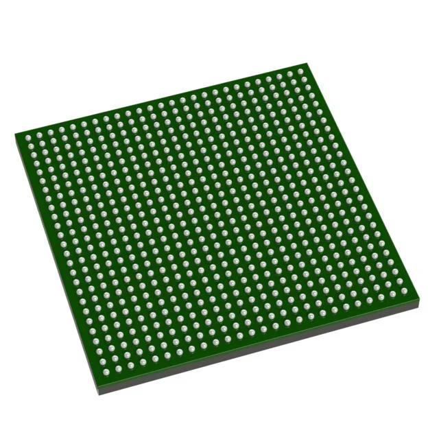
Технические характеристики
Part Number Explanation
This is a wide-temperature industrial-grade mid-density FPGA belonging to Xilinx Kintex-7 family, built on mature 28nm process technology. It delivers balanced logic performance, abundant I/O expandability and stable low power consumption, targeted at industrial automation, wired communication and portable test devices working under harsh wide-temperature environments.
- XC7K70T: Mid-range density chip of Kintex-7 series, T stands for low-power optimized version
- -2: Speed Grade 2, mainstream balanced timing grade. It reserves sufficient timing allowance for most industrial digital logic designs, striking a balance between operating frequency, timing stability and overall power consumption
- FBG676: 676-ball flip-chip BGA package, larger pin count brings more configurable user I/O resources for multi-peripheral extended design
- E: Extended industrial temperature grade, operating junction temperature range: -40°C ~ +100°C
On-Chip Hardware Resource Details
1. General Logic Resources
- Total Logic Cells: 70800
- Available Slices: 11060
- Total Flip-Flops: 88480
- Total LUTs: 44240
2. Arithmetic and Storage Resources
- DSP48E1 arithmetic units: 240 units, used for FFT computation, digital filtering, motor control algorithms, signal convolution and mathematical operation acceleration
- Total Block RAM capacity: 3780 Kb, applied for data buffering, FIFO queues and local parameter storage
- Distributed RAM capacity: 1188 Kb
3. Clock Management Resources
- 6 MMCM clock management tiles
- 6 PLL phase-locked loops
Supports multi-domain clock generation, clock phase adjustment and high-frequency jitter suppression to meet synchronous timing demands of multi-module systems
4. Высокоскоростные последовательные приемопередатчики
- 8 channels of GTX high-speed serial transceivers
Maximum line rate reaches 6.6Gbps, compatible with PCIe Gen2, Aurora, CPRI, Gigabit Ethernet and other mainstream serial communication protocols
5. Интерфейсы ввода-вывода и встроенный модуль мониторинга
- Настраиваемые выводы ввода-вывода пользователя: 400
I/O bank voltage adjustable from 1.2V to 3.3V, fully compatible with LVCMOS, LVDS, HSTL and common differential signal standards
Dual-channel 12-bit XADC analog monitor is integrated on chip, realizing real-time detection of die junction temperature, internal power supply voltages and external analog input signals
Технические характеристики источника питания
Nominal core internal voltage: 1.0V
Independent power domains are configured for logic area, block RAM and high-speed transceivers respectively
Typical overall power consumption: 3.5W ~ 13W; passive heat dissipation can fulfill long-term continuous operation requirements under conventional industrial loads
Packaging & SMT Assembly Requirements
- Package type: 676-pin FCBGA flip-chip ball grid array
- Moisture Sensitivity Level: MSL3; all reflow soldering procedures must be completed within 168 hours after vacuum packaging is opened
- Lead-free structure, fully compliant with RoHS environmental directives
- Delivered and stored in anti-static trays for automated PCB mass production
Приспособляемость к условиям окружающей среды и надежность
The chip can operate stably and continuously under wide temperature fluctuations, mechanical vibration and moderate electromagnetic interference industrial environments. It supports bitstream encryption protection and SEU single-event upset error detection, featuring strong anti-interference and high operational reliability for field rugged devices.
Типичные сценарии применения
- Multi-axis industrial motion controllers, servo drive main control boards
- Industrial Ethernet converters, multi-channel fieldbus protocol gateway modules
- Portable vibration acquisition analyzers, on-site environmental monitoring terminals
- Small base station baseband auxiliary processing boards, wireless signal forwarding units
- Medical device data acquisition and logic control modules
- Wide-temperature industrial core boards and embedded algorithm verification platforms


