






| MÃ SẢN PHẨM | BỘ PHIM | SỐ LƯỢNG PHÒNG THÍ NGHIỆM/CLBS | ĐỘ BỀN THEO TỐC ĐỘ | SỐ LƯỢNG PHẦN TỬ LỐI / TẾ BÀO | Tổng số bit RAM | SỐ LƯỢNG I/O | Điện áp – Nguồn cấp | Loại lắp đặt | NHIỆT ĐỘ HOẠT ĐỘNG | GÓI / HỘP | GÓI THIẾT BỊ CỦA NHÀ CUNG CẤP |
|---|---|---|---|---|---|---|---|---|---|---|---|
| XC7K70T-2FBG676E | Kintex-7 | 5.125,00 | -2,00 | 65,600 | 4976640 | 300 | 0,97 – 1,03 V (thông thường 1,0 V) | Lắp đặt bề mặt | 0 °C — 100 °C | FBG-676 (27×27 mm) | 676-FCBGA |
XC7K70T-2FBG676E
Nhà sản xuất: Xilinx
Tế bào logic: 70,400
Các lát cắt logic: 11,000
Bộ nhớ RAM tích hợp (eRAM): 4.680 Kb (130 khối RAM 36 Kb)
Dung lượng I/O tối đa của người dùng: 400
Gói: FBG676 (BGA lật chip)
Đánh giá tốc độ: -2
Nhiệt độ hoạt động: Mở rộng (0°C đến +100°C)
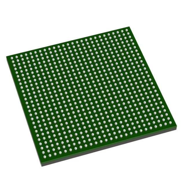
Thông số kỹ thuật
Giải thích về mã sản phẩm
This is a wide-temperature industrial-grade mid-density FPGA belonging to Xilinx Kintex-7 family, built on mature 28nm process technology. It delivers balanced logic performance, abundant I/O expandability and stable low power consumption, targeted at industrial automation, wired communication and portable test devices working under harsh wide-temperature environments.
- XC7K70T: Mid-range density chip of Kintex-7 series, T stands for low-power optimized version
- -2: Speed Grade 2, mainstream balanced timing grade. It reserves sufficient timing allowance for most industrial digital logic designs, striking a balance between operating frequency, timing stability and overall power consumption
- FBG676: 676-ball flip-chip BGA package, larger pin count brings more configurable user I/O resources for multi-peripheral extended design
- E: Loại chịu nhiệt độ công nghiệp mở rộng, dải nhiệt độ điểm nối hoạt động: -40°C ~ +100°C
On-Chip Hardware Resource Details
1. General Logic Resources
- Total Logic Cells: 70800
- Available Slices: 11060
- Total Flip-Flops: 88480
- Total LUTs: 44240
2. Arithmetic and Storage Resources
- DSP48E1 arithmetic units: 240 units, used for FFT computation, digital filtering, motor control algorithms, signal convolution and mathematical operation acceleration
- Total Block RAM capacity: 3780 Kb, applied for data buffering, FIFO queues and local parameter storage
- Distributed RAM capacity: 1188 Kb
3. Clock Management Resources
- 6 MMCM clock management tiles
- 6 PLL phase-locked loops
Supports multi-domain clock generation, clock phase adjustment and high-frequency jitter suppression to meet synchronous timing demands of multi-module systems
4. Bộ thu phát nối tiếp tốc độ cao
- 8 channels of GTX high-speed serial transceivers
Maximum line rate reaches 6.6Gbps, compatible with PCIe Gen2, Aurora, CPRI, Gigabit Ethernet and other mainstream serial communication protocols
5. I/O Interfaces and On-Chip Monitoring Module
- Configurable user I/O pins: 400
I/O bank voltage adjustable from 1.2V to 3.3V, fully compatible with LVCMOS, LVDS, HSTL and common differential signal standards
Dual-channel 12-bit XADC analog monitor is integrated on chip, realizing real-time detection of die junction temperature, internal power supply voltages and external analog input signals
Thông số kỹ thuật bộ nguồn
Nominal core internal voltage: 1.0V
Independent power domains are configured for logic area, block RAM and high-speed transceivers respectively
Typical overall power consumption: 3.5W ~ 13W; passive heat dissipation can fulfill long-term continuous operation requirements under conventional industrial loads
Yêu cầu về đóng gói và lắp ráp SMT
- Package type: 676-pin FCBGA flip-chip ball grid array
- Moisture Sensitivity Level: MSL3; all reflow soldering procedures must be completed within 168 hours after vacuum packaging is opened
- Cấu trúc không chứa chì, tuân thủ hoàn toàn các chỉ thị môi trường RoHS
- Delivered and stored in anti-static trays for automated PCB mass production
Environmental Adaptability and Reliability
The chip can operate stably and continuously under wide temperature fluctuations, mechanical vibration and moderate electromagnetic interference industrial environments. It supports bitstream encryption protection and SEU single-event upset error detection, featuring strong anti-interference and high operational reliability for field rugged devices.
Các tình huống ứng dụng điển hình
- Multi-axis industrial motion controllers, servo drive main control boards
- Industrial Ethernet converters, multi-channel fieldbus protocol gateway modules
- Portable vibration acquisition analyzers, on-site environmental monitoring terminals
- Small base station baseband auxiliary processing boards, wireless signal forwarding units
- Medical device data acquisition and logic control modules
- Wide-temperature industrial core boards and embedded algorithm verification platforms


