






| MODELO P/N | SERIE | NÚMERO DE LABORATORIOS/CLBS | GRADO DE VELOCIDAD | NÚMERO DE ELEMENTOS LÓGICOS / CELDAS | TOTAL BITS RAM | NÚMERO DE E/S | TENSIÓN - ALIMENTACIÓN | TIPO DE MONTAJE | TEMPERATURA DE FUNCIONAMIENTO | PAQUETE / ESTUCHE | PAQUETE DEL DISPOSITIVO DEL PROVEEDOR |
|---|---|---|---|---|---|---|---|---|---|---|---|
| XCKU3P-3SFVB784E | Kintex® UltraScale+ | 20,34 | -3,00 | 355 950 LE | 31641600 | 304 | 0,873 V ~ 0,927 V | Montaje en superficie | 0 °C ~ +100 °C (grado E) | 784-FCBGA | 784-FCBGA |
XCKU3P-3SFVB784E
Fabricante: Xilinx
Células lógicas: 3,780,000
Rebanadas lógicas: 590,000
RAM integrada (eRAM): 81 360 Kb (2260 bloques de RAM de 36 Kb)
E/S máxima por usuario: 400
Paquete: SFVB784 (BGA con chip invertido)
Grado de velocidad: -3
Temperatura de funcionamiento: Ampliado (0 °C a +100 °C)
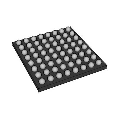
Especificaciones
Explicación del número de pieza
This is AMD Xilinx Kintex UltraScale+ series low-power mid-range FPGA built on 16nm FinFET process, optimized for cost-sensitive embedded systems, portable signal processing and low-latency edge applications.
- XCKU3P: Entry-level Kintex UltraScale+ device with reduced power consumption
- -3: Speed Grade 3, power-optimized timing grade, prioritizes low power consumption over maximum operating frequency
- SFVB784: 784-ball flip-chip FCBGA compact package
- E: Grado de temperatura industrial ampliado, rango de temperatura de unión: -40 °C a +125 °C
Recursos de hardware del núcleo en el chip
Logic & DSP Units
- Total Logic Cells: 221,280
- DSP48E2 dedicated arithmetic blocks: 1128 units
Used for digital filtering, FFT computation, sensor data processing, lightweight image algorithms and small-scale matrix calculations
Memoria integrada
- Total Block RAM capacity: 14.5 Mb
Composed of independent 36K dual-port RAM banks for data buffering, FIFO storage and intermediate algorithm data caching
Distributed RAM implemented via LUT resources for ultra-low latency small temporary storage
Módulos de gestión de reloj
Integrated multiple MMCM and PLL clock management tiles. Capable of clock multiplication, division, arbitrary phase offset adjustment and jitter attenuation to satisfy multi-clock domain system design demands
High-Speed Transceivers & General I/O
- 8 GTH serial transceivers, maximum single lane rate up to 16.375 Gbps
Supports PCIe Gen3, Aurora, JESD204B, 10G Ethernet and other high-speed serial protocols
- Available user I/O pins: 324
Equipped with HR wide-voltage I/O banks and HP high-speed I/O banks; supports LVCMOS, LVDS, HSTL, SSTL and mainstream differential signaling standards
- Built-in SYSMON system monitor: tracks chip internal temperature, power supply voltages and external analog input signals in real time
Especificaciones de la fuente de alimentación
Nominal core logic voltage: 0.85 V
Separate independent power domains are arranged for core logic, memory modules, transceivers and I/O interfaces. Dynamic voltage and frequency adjustment is supported to cut power consumption under light load.
Typical total power consumption: 9W ~ 28W, passive heat sink cooling is feasible for compact embedded hardware
Requisitos de empaque y ensamblaje SMT
- Paquete: FCBGA (matriz de bolas) de 784 pines con tecnología flip-chip
- Moisture Sensitivity Level: MSL3; all reflow soldering operations must be completed within 168 hours after vacuum packaging is opened
- Lead-free design, fully compliant with RoHS environmental regulations
- Delivered in anti-static trays for automated industrial PCB mass production
Environmental and Reliability Features
Stable continuous operation is guaranteed under extreme temperature fluctuations and strong electromagnetic interference environments.
It supports 256-bit AES bitstream encryption for intellectual property protection, SEU radiation error correction and partial dynamic reconfiguration, perfectly suited for automotive electronics, outdoor industrial terminals and portable airborne equipment requiring high reliability.
Escenarios típicos de aplicación
- Portable software-defined radio, miniature wireless signal transceiving and baseband preprocessing modules
- Embedded machine vision terminals, industrial portable defect inspection equipment
- Multi-channel portable data recorders, vibration monitoring and handheld precision measuring instruments
- Automotive peripheral control units, vehicle-mounted video preprocessing modules
- Miniature airborne signal acquisition and short-range radar front-end processing boards
- Low-cost PCIe data acquisition cards and custom embedded core system boards


