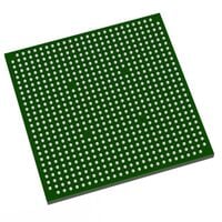
| MODELO P/N | SERIE | NÚMERO DE LABORATORIOS/CLBS | GRADO DE VELOCIDAD | NÚMERO DE ELEMENTOS LÓGICOS / CELDAS | TOTAL BITS RAM | NÚMERO DE E/S | TENSIÓN - ALIMENTACIÓN | TIPO DE MONTAJE | TEMPERATURA DE FUNCIONAMIENTO | PAQUETE / ESTUCHE | PAQUETE DEL DISPOSITIVO DEL PROVEEDOR |
|---|---|---|---|---|---|---|---|---|---|---|---|
| XC4VLX40-10FFG668C | Virtex-4 LX | 4.608,00 | -10,00 | 41472 | 1769472 | 448 | 1,14 V ~ 1,26 V | Montaje en superficie | 0 °C ~ +85 °C (Commercial) | 668-BBGA (FCBGA) | 668-FCBGA |
XC4VLX200-10FFG1513C: High-Capacity Logic Integration for Commercial Computing Platforms
En XC4VLX40-10FFG668C is a high-performance member of the Xilinx Virtex®-4 LX family, optimized for logic-intensive commercial applications. Built on the proven 90nm ASMBL™ (Advanced Silicon Modular Block) architecture, this FPGA delivers a robust 41k logic cell fabric that bridges the gap between low-cost entry-level chips and high-end workstation-class silicon.
Housed in the FFG668 Lead-Free package, it provides a versatile I/O-to-logic ratio, making it the ideal choice for high-speed data bridging, localized signal processing, and system-level control.
Core Engineering Highlights
Efficient Logic Density: With 41,472 Logic Cells, this device is tailored for designs that require complex state machines and custom RTL without the power overhead of oversized FPGAs.
XtremeDSP™ Capability: Includes 64 dedicated DSP48 slices. These hard-coded blocks allow for high-speed arithmetic (up to 400MHz+) without taxing the general-purpose logic fabric, perfect for real-time filtering and digital modulation.
Optimized Memory Hierarchy: Equipped with 1,728 Kb of Block RAM (BRAM). The dual-port nature of this memory is essential for implementing high-speed FIFOs and local data caching in streaming applications.
Superior Signal Integrity: En FFG668 package offers 448 User I/Os. The Flip-Chip (FFG) technology minimizes parasitic inductance, reducing Simultaneous Switching Noise (SSN)—a critical factor when driving high-speed parallel buses like DDR2 or QDR SRAM.
Digital Clock Management (DCM): Features advanced clocking resources that provide sub-nanosecond skew control and frequency synthesis, ensuring stable timing closure across the entire 668-pin array.
Technical Specification Matrix
| Característica | Especificación |
| Células lógicas | 41,472 |
| CLB Array | 4,608 |
| Bloque total RAM | 1,728 Kb |
| DSP48 Slices | 64 |
| Max User I/O | 448 |
| Grado de velocidad | -10 (Standard Performance) |
| Paquete | FFG668 (Lead-Free / 1.0mm Pitch) |
| Grado de temperatura | Comercial (0°C a +85°C) |


