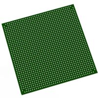
| MODELO P/N | SERIE | NÚMERO DE LABORATORIOS/CLBS | GRADO DE VELOCIDAD | NÚMERO DE ELEMENTOS LÓGICOS / CELDAS | TOTAL BITS RAM | NÚMERO DE E/S | TENSIÓN - ALIMENTACIÓN | TIPO DE MONTAJE | TEMPERATURA DE FUNCIONAMIENTO | PAQUETE / ESTUCHE | PAQUETE DEL DISPOSITIVO DEL PROVEEDOR |
|---|---|---|---|---|---|---|---|---|---|---|---|
| XC4VLX200-11FFG1513C | Virtex-4 LX | 22.272,00 | -11,00 | 200448 | 6193152 | 960 | 1,14 V ~ 1,26 V | Montaje en superficie | 0 °C ~ +85 °C (Commercial) | 1513-BBGA (FCBGA) | 1513-FCBGA |
XC4VLX200-11FFG1513C: The Performance Pinnacle of High-Density Logic Integration
En XC4VLX200-11FFG1513C is the highest-specification, high-density FPGA in the Xilinx Virtex®-4 LX family. Built on the 90nm ASMBL™ (Advanced Silicon Modular Block) architecture, this device is engineered for architects who require the absolute maximum logic capacity paired with the superior -11 speed grade. It is the industry-standard choice for complex, logic-heavy applications where timing closure and single-chip integration are critical.
Featuring a staggering 200,448 Logic Cells and the fastest commercial speed grade, the LX200-11 is designed to push the boundaries of real-time data processing and large-scale system emulation.
Key Engineering Advantages
Fastest Timing Closure (-11 Speed Grade): The -11 speed grade is essential for high-performance designs, providing a significant frequency boost over the standard -10 models. This extra headroom is vital for stabilizing 300MHz+ internal logic fabrics and high-speed memory interfaces.
Massive Logic Consolidation: With over 200k logic cells, this FPGA allows for the integration of entire multi-processor systems, complex encryption engines, and massive state machines into a single die, eliminating the latency and complexity of multi-chip partitioning.
Unrivaled I/O Capacity: Housed in the FFG1513 package, the device provides 960 User I/Os. This allows for massive parallel throughput, easily supporting multiple wide-bus interfaces like DDR2/QDR-II and high-speed backplane protocols.
High-Performance DSP & Memory: Includes 6,048 Kb of Block RAM y 96 XtremeDSP™ slices. The combination of dense memory and dedicated arithmetic hardware makes it a powerhouse for real-time signal processing and 4K video algorithms.
RoHS Compliant Flip-Chip Packaging: En FFG1513 package is optimized for both environmental compliance and thermal integrity. Its design ensures low-inductance power delivery and superior heat dissipation, even at high switching frequencies.
Technical Specification Matrix
| Característica | Especificación |
| Células lógicas | 200,448 |
| CLB Array | 22,512 |
| Bloque total RAM | 6,048 Kb |
| DSP48 Slices | 96 |
| Max User I/O | 960 |
| Grado de velocidad | -11 (High Performance) |
| Grado de temperatura | Comercial (0°C a +85°C) |
| Paquete | FFG1513 (Lead-Free / 1.0mm Pitch) |
Why Specify the LX200-11C?
1. Solving the Routing Congestion Challenge
In many high-density designs, routing congestion can kill timing. The Virtex-4 ASMBL architecture in the LX200 ensures a highly uniform distribution of logic, memory, and I/O. Combined with the -11 speed grade, this allows for much easier timing closure on designs that utilize 85% or more of the available logic resources.
2. Signal Integrity at Scale
Driving nearly 1,000 I/Os simultaneously requires a robust power distribution network. The FFG1513 package is specifically designed with an extensive array of VCC and GND pins to suppress Simultaneous Switching Noise (SSN), ensuring clean signal eyes for high-speed differential and single-ended signaling.
3. Long-Lifecycle Stability
The LX200-11C is a proven, mature platform. For mission-critical commercial systems—such as high-end medical scanners or broadcasting switchers—the stability of the Virtex-4 toolchain and the known reliability of the 90nm process provide a low-risk path to production.
Aplicaciones de destino
ASIC/SoC Prototyping: Large-scale logic verification and pre-silicon emulation.
Professional Video Gear: Real-time 8K/4K image reconstruction and conversion.
Telecommunications: High-bandwidth switching fabrics and protocol acceleration.
Advanced Instrumentation: High-speed data acquisition and real-time analysis for scientific research.


