






| MODELL P/N | SERIE | ANZAHL DER LABORE/KLINIKEN | GESCHWINDIGKEITSSTUFE | ANZAHL DER LOGIKELEMENTE / ZELLEN | RAM-BITS INSGESAMT | ANZAHL DER E/A | SPANNUNG - VERSORGUNG | BEFESTIGUNGSTYP | BETRIEBSTEMPERATUR | VERPACKUNG / KASSE | LIEFERANT GERÄTEPAKET |
|---|---|---|---|---|---|---|---|---|---|---|---|
| XC6VLX240T-L1FF784C | Virtex-6 LXT | 0,00 | 18.840,00 | 241,152 | 15335424 | 400 | 0.95 - 1.05 V | Oberflächenmontage | 0°C - 85°C (C) | FCBGA-784 | 784-FCBGA |
XC6VLX240T-L1FF784C
Hersteller: Xilinx
Logische Zellen: 241,152
Logische Schnitte: 37,680
Eingebettetes RAM (eRAM): 14.976 Kb (832 × 18 Kb Block-RAM)
Maximale Benutzer-E/A: 360
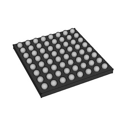
Paket: FF784 (Flip-Chip BGA)
Geschwindigkeitsstufe: -1L
Betriebstemperatur: Handelsüblich (0°C bis +85°C)
Spezifikationen
Definition der Artikelnummer
This commercial low-power FPGA belongs to Xilinx Virtex-6 LX family, manufactured on advanced 40nm low-power CMOS process. LX series focuses on abundant general logic resources, ideal for general digital system design, logic control and interface conversion scenarios.
- XC6VLX240T: Mid-large capacity logic-oriented Virtex-6 device, rich programmable logic cells for complex sequential and combinational logic development, widely used in industrial control, data acquisition and protocol conversion systems
- L1: Low power grade 1, ultra-low static power specification. Power consumption reduction is the primary priority over maximum operating frequency, designed for continuously running indoor equipment with strict heat dissipation limitations
- FF784: 784-pin flip-chip BGA package, compact overall size, balanced heat dissipation and signal integrity. Pin resources fully support GTX transceivers, user I/O and DDR3 memory peripheral layout
- C: Commercial temperature range, junction temperature operating range: 0°C ~ +85°C
On-Chip Hardware Resource Parameters
1. Programmierbare Logikressourcen
- Total System Logic Cells: 241,152
- Available CLB Slices: 37,680
- Total Flip-Flops: 753,600
- Total LUTs: 376,800
- Distributed RAM: 3.89 Mb
2. Arithmetic & Embedded Memory Resources
- DSP48E1 arithmetic units: 768 units, applicable to basic digital filtering, simple FFT calculation, low-speed signal processing and auxiliary computing tasks
- Total Block RAM Capacity: 18.7 Mb, used for data buffering, FIFO cache, configuration parameter storage and small image frame caching
3. Clock Management Subsystem
- 12 Clock Management Tiles (CMT)
Each CMT consists of one MMCM and one PLL. Multiple independent clock domains can be configured flexibly, supporting clock delay compensation, phase adjustment and low-jitter clock generation to meet timing demands of multi-clock digital systems
4. Serielle Hochgeschwindigkeits-Transceiver
- 12 GTX differential high-speed transceivers
Max single lane rate: 6.25 Gbps, compatible with PCIe Gen2, Aurora, JESD204, Serial RapidIO and common high-speed board-to-board transmission protocols
5. I/O Interfaces & Monitoring Module
- Configurable user I/O pins: 400
Supports I/O voltage from 1.2V to 3.3V, compatible with LVCMOS, LVDS, HSTL, SSTL and all mainstream single-ended and differential signal standards
Built-in analog monitoring circuit continuously detects chip internal temperature, core supply voltage and external analog signals in real time
Power Supply Characteristics
Core voltage is optimized for low power consumption. Logic array, block RAM, DSP modules and serial transceivers are divided into independent power domains, allowing partial power gating to cut idle power consumption dynamically
Typical overall power consumption: 9W ~ 26W. Continuous full-load operation at maximum commercial temperature needs forced air cooling
Packaging and SMT Assembly Specifications
- Package: 784-ball Flip-Chip BGA
- Moisture Sensitivity Level: MSL4; all reflow soldering must be finished within 72 hours once vacuum package is unsealed
- Lead-free design, compliant with RoHS requirements
- Products are stored and delivered with anti-static packaging to prevent electrostatic damage during PCB assembly
Umgebungsanpassungsfähigkeit und Zuverlässigkeit
This chip is dedicated to stable indoor constant-temperature environments. It runs reliably under tiny temperature variations, mild vibration and conventional electromagnetic interference. It supports bitstream encryption, dynamic partial reconfiguration and SEU error checking. Without radiation-hardened design, it cannot work stably in outdoor low-temperature, vehicle vibration and aerospace harsh environments.
Typische Anwendungsszenarien
- Industrial multi-channel data acquisition main control boards and factory automation logic control platforms
- Laboratory medium-speed signal test equipment and protocol conversion gateway hardware
- Embedded high-speed storage front-end control modules and image preprocessing equipment
- Small-scale digital system prototype verification and teaching experimental development boards
- Communication auxiliary interface boards and wired transmission signal switching devices


