






| MÃ SẢN PHẨM | BỘ PHIM | SỐ LƯỢNG PHÒNG THÍ NGHIỆM/CLBS | ĐỘ BỀN THEO TỐC ĐỘ | SỐ LƯỢNG PHẦN TỬ LỐI / TẾ BÀO | Tổng số bit RAM | SỐ LƯỢNG I/O | Điện áp – Nguồn cấp | Loại lắp đặt | NHIỆT ĐỘ HOẠT ĐỘNG | GÓI / HỘP | GÓI THIẾT BỊ CỦA NHÀ CUNG CẤP |
|---|---|---|---|---|---|---|---|---|---|---|---|
| XCKU3P-1FFVB676C | Kintex® UltraScale+ | 20,34 | -1,00 | 355.950 LE | 31.641.600 bit | 272 | 0,850 V | Lắp đặt bề mặt | -40 °C – 100 °C | FCBGA-676 | 676-FCBGA (27×27) |
XCKU3P-1FFVB676C
Nhà sản xuất: Xilinx
Tế bào logic: 3,780,000
Các lát cắt logic: 590,000
Bộ nhớ RAM tích hợp (eRAM): 81.360 Kb (2.260 × 36 Kb bộ nhớ RAM khối)
Dung lượng I/O tối đa của người dùng: 350
Gói: FFVB676 (BGA lật chip)
Đánh giá tốc độ: -1
Nhiệt độ hoạt động: Thương mại (0°C đến +85°C)
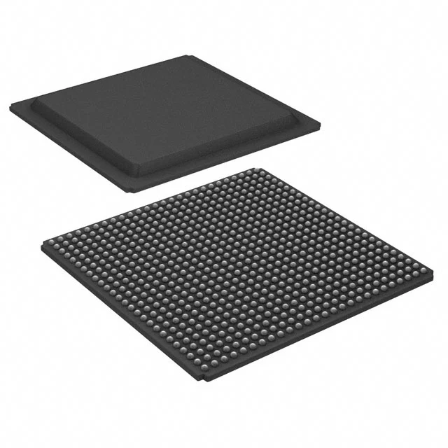
Thông số kỹ thuật
Phân tích mã sản phẩm
This is Xilinx Kintex UltraScale+ series FPGA manufactured on 16nm FinFET process, equipped with built-in UltraRAM large-capacity on-chip memory, positioned for cost-sensitive commercial embedded high-speed logic and data processing applications.
- XCKU3P: Entry-level chip of Kintex UltraScale+ P variant family
- -1: Speed Grade 1, the slowest timing grade for this device, optimized for cost reduction rather than high-frequency operation
- FFVB676: 676-ball flip-chip FCBGA compact package
- C: Commercial temperature grade, junction temperature range: 0°C ~ +85°C
On-Chip Hardware Resources
Logic & DSP Resources
- Tổng số ô logic: 221.280
- Các khối tính toán chuyên dụng của DSP48E2: 1.128 đơn vị
Suitable for digital filtering, FFT calculation, low-speed wireless baseband processing, basic image algorithm acceleration and small matrix computing tasks
Bộ nhớ nhúng
- Total Block RAM: 14.5 Mb
- Dedicated UltraRAM memory: 13.5 Mb, used for video frame buffers, deep data buffering and intermediate storage of large algorithms
- LUT-implemented distributed RAM for ultra-low latency tiny temporary cache
Clock Management Subsystem
Multiple MMCM and PLL clock management tiles are integrated. Functions include clock multiplication, division, arbitrary phase adjustment and jitter suppression to meet timing requirements of multi-clock digital systems.
Bộ thu phát tốc độ cao & Giao diện I/O chung
- 8 GTH high-speed serial transceivers, maximum per-lane rate up to 16.375 Gbps
Supported protocols: PCIe Gen3, 10G Ethernet, JESD204B/C, Aurora
- Usable user I/O pins: 280
Adopts HR wide-voltage I/O banks and HP high-performance I/O banks, compatible with LVCMOS, LVDS, HSTL, SSTL and all mainstream differential signaling standards
- Onboard SYSMON system monitor: Real-time monitoring of chip internal temperature, power supply voltages and external analog input signals
Thông số kỹ thuật bộ nguồn
Nominal core operating voltage: 0.85 V
Independent power domains are configured for core logic, memory modules, transceivers and I/O interfaces. Dynamic voltage and frequency scaling can be enabled to decrease power consumption under light load conditions.
Typical overall power consumption: 9W ~ 28W, passive heat dissipation works well for compact commercial embedded devices
Packaging & SMT Assembly Rules
- Package: 676-pin flip-chip FCBGA ball grid array
- Moisture Sensitivity Level: MSL3; reflow soldering must be completed within 168 hours after vacuum packaging is opened
- Lead-free design, fully compliant with RoHS standards
- Delivered in anti-static trays for automated PCB mass production
Environmental & Reliability Characteristics
Only applicable to indoor stable commercial ambient environments, unable to adapt to outdoor extreme temperature industrial scenarios.
It supports 256-bit AES bitstream encryption for IP protection, SEU single-event upset error correction and partial dynamic reconfiguration, offering stable performance for indoor test instruments, commercial vision equipment and desktop data acquisition devices.
Các tình huống ứng dụng điển hình
- Indoor small cell communication equipment, compact network forwarding and gateway modules
- Desktop laboratory multi-channel image acquisition and simple visual inspection platforms
- Bench signal analyzers, portable laboratory measuring instruments and multi-channel data recorders
- Low-cost PCIe high-speed acquisition cards and algorithm prototype verification boards
- Commercial video real-time processing, multi-channel video decoding and playback terminals
- Custom embedded core boards for secondary development in commercial electronic products


