






| МОДЕЛЬ П/Н | СЕРИИ | КОЛИЧЕСТВО ЛАБОРАТОРИЙ/КЛБ | УРОВЕНЬ СКОРОСТИ | КОЛИЧЕСТВО ЛОГИЧЕСКИХ ЭЛЕМЕНТОВ / ЯЧЕЕК | ВСЕГО БИТОВ ОЗУ | КОЛИЧЕСТВО ВХОДОВ/ВЫХОДОВ | НАПРЯЖЕНИЕ - ПИТАНИЕ | ТИП КРЕПЛЕНИЯ | РАБОЧАЯ ТЕМПЕРАТУРА | УПАКОВКА / КЕЙС | УПАКОВКА УСТРОЙСТВА ПОСТАВЩИКА |
|---|---|---|---|---|---|---|---|---|---|---|---|
| XC7K480T-2FFG901E | Kintex-7 | 37.325,00 | -2,00 | 477,760 | 35205120 | 380 | 0.97 - 1.03 | Монтаж на поверхность | 0 °C ... +100 °C (E) | FCBGA-901 (FFG901) | 901-FCBGA (31×31) |
XC7K480T-2FFG901E
Производитель: Xilinx
Логические ячейки: 477,760
Логические срезы: 74,650
Встроенная оперативная память (eRAM): 33 840 Кб (940 × 36 Кб блочной оперативной памяти)
Максимальный пользовательский ввод/вывод: 400
Упаковка: FFG901 (Flip-Chip BGA)
Класс скорости: -2
Рабочая температура: Расширенный (от 0°C до +100°C)
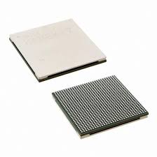
Технические характеристики
Определение номера детали
This is a large-capacity extended industrial temperature FPGA from Xilinx Kintex-7 series, built on proven 28nm semiconductor manufacturing process. It integrates abundant logic, DSP and embedded memory resources inside a compact footprint package, optimized for miniaturized rugged embedded devices that demand powerful parallel computing capability, wide-temperature stability and limited equipment installation space.
- XC7K480T: Top-tier high-density model of Kintex-7 family; the suffix T denotes low-power optimized silicon die
- -2: Speed Grade 2, the most widely adopted balanced timing grade. It reserves sufficient timing margin for large-scale high-frequency digital circuit design, striking an optimal balance between maximum operating frequency, timing closure reliability and overall power consumption
- FFG901: 901-ball flip-chip FCBGA compact package. Smaller overall size facilitates hardware miniaturization design while retaining adequate I/O and peripheral expansion resources
- E: Extended industrial temperature range, operating junction temperature: -40°C ~ +100°C
Параметры аппаратных ресурсов на кристалле
1. General Programmable Logic Resources
- Total Logic Cells: 485,760
- Configurable Slices: 75,900
- Total Flip-Flops: 607,200
- Total LUTs: 303,600
2. Arithmetic and Memory Resources
- DSP48E1 arithmetic units: 1,920 pieces, applicable to massive FFT operations, digital filtering, radar signal demodulation, multi-channel HD video algorithm acceleration and large matrix mathematical calculations
- Total Block RAM capacity: 34,290 Kb, used for image frame buffering, deep FIFO data caching, waveform storage and algorithm parameter lookup tables
- Distributed RAM capacity: 8,440 Kb
3. Подсистема управления часами
- 12 MMCM clock management tiles
- 12 PLL phase-locked loops
Supports multi-clock domain generation, phase fine adjustment, clock delay compensation and high-frequency clock jitter suppression, satisfying strict synchronous timing requirements of ultra-large complex digital systems
4. Высокоскоростные последовательные приемопередатчики
- 20 GTX high-speed differential transceivers
Maximum line rate reaches 10.3125 Gbps, compatible with PCIe Gen2, 10 Gigabit Ethernet, CPRI, JESD204B, Aurora and other mainstream high-speed serial communication protocols
5. I/O Interfaces & On-Chip Monitoring Module
- User configurable I/O pins: 444
I/O bank voltage can be configured from 1.2V to 3.3V, fully supporting LVCMOS, LVDS, HSTL, SSTL and all mainstream differential signal standards
A dual-channel 12-bit XADC analog monitor is embedded on the chip, realizing real-time continuous monitoring of die junction temperature, all internal power supply voltages and external analog input signals
Технические характеристики источника питания
Nominal core logic operating voltage: 1.0V
Independent isolated power domains are set for logic fabric, Block RAM, DSP array and high-speed transceivers separately
Typical overall power consumption: 13W ~ 38W. Compact forced-air active cooling is required to maintain stable full-load operation under maximum temperature working conditions
Packaging & SMT Assembly Requirements
- Package form: 901-pin flip-chip FCBGA ball grid array
- Moisture Sensitivity Level: MSL4; all reflow soldering procedures must be finished within 72 hours after vacuum packaging is opened
- Lead-free packaging structure, fully compliant with RoHS environmental directives
- Stored and shipped in anti-static trays to avoid electrostatic damage during automated PCB mass production
Environmental Adaptability & Reliability
The chip can operate continuously and stably under severe temperature fluctuations, mechanical vibration, impact and moderate electromagnetic interference harsh industrial environments. It supports 256-bit AES bitstream encryption protection and SEU single-event upset detection and correction, with outstanding thermal robustness and anti-interference performance for long-term field deployment.
Типичные сценарии применения
- Portable high-end spectrum analyzers, multi-channel high-speed oscilloscopes and transient signal recording devices
- Software-defined radio baseband processing units, miniaturized outdoor wireless communication main control boards
- Multi-channel industrial machine vision inspection systems, compact high-speed real-time image processing terminals
- Vehicle-mounted multi-sensor fusion computing hosts, automotive intelligent edge control equipment
- Light airborne radar signal preprocessing modules, flight data acquisition and forwarding units
- Wide-temperature high-performance industrial SOM core boards and ultra-complex embedded algorithm prototype verification platforms


