






| MÃ SẢN PHẨM | BỘ PHIM | SỐ LƯỢNG PHÒNG THÍ NGHIỆM/CLBS | ĐỘ BỀN THEO TỐC ĐỘ | SỐ LƯỢNG PHẦN TỬ LỐI / TẾ BÀO | Tổng số bit RAM | SỐ LƯỢNG I/O | Điện áp – Nguồn cấp | Loại lắp đặt | NHIỆT ĐỘ HOẠT ĐỘNG | GÓI / HỘP | GÓI THIẾT BỊ CỦA NHÀ CUNG CẤP |
|---|---|---|---|---|---|---|---|---|---|---|---|
| XC7K480T-2FFG901E | Kintex-7 | 37.325,00 | -2,00 | 477,760 | 35205120 | 380 | 0,97 – 1,03 | Lắp đặt bề mặt | 0 °C … +100 °C (E) | FCBGA-901 (FFG901) | 901-FCBGA (31×31) |
XC7K480T-2FFG901E
Nhà sản xuất: Xilinx
Tế bào logic: 477,760
Các lát cắt logic: 74,650
Bộ nhớ RAM tích hợp (eRAM): 33.840 Kb (940 × 36 Kb bộ nhớ RAM khối)
Dung lượng I/O tối đa của người dùng: 400
Gói: FFG901 (BGA lật chip)
Đánh giá tốc độ: -2
Nhiệt độ hoạt động: Mở rộng (0°C đến +100°C)
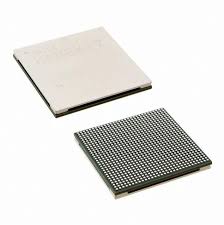
Thông số kỹ thuật
Định nghĩa mã sản phẩm
This is a large-capacity extended industrial temperature FPGA from Xilinx Kintex-7 series, built on proven 28nm semiconductor manufacturing process. It integrates abundant logic, DSP and embedded memory resources inside a compact footprint package, optimized for miniaturized rugged embedded devices that demand powerful parallel computing capability, wide-temperature stability and limited equipment installation space.
- XC7K480T: Top-tier high-density model of Kintex-7 family; the suffix T denotes low-power optimized silicon die
- -2: Speed Grade 2, the most widely adopted balanced timing grade. It reserves sufficient timing margin for large-scale high-frequency digital circuit design, striking an optimal balance between maximum operating frequency, timing closure reliability and overall power consumption
- FFG901: 901-ball flip-chip FCBGA compact package. Smaller overall size facilitates hardware miniaturization design while retaining adequate I/O and peripheral expansion resources
- E: Dải nhiệt độ công nghiệp mở rộng, nhiệt độ điểm nối hoạt động: -40°C ~ +100°C
Các tham số tài nguyên phần cứng trên chip
1. Các tài nguyên chung về logic lập trình được
- Tổng số ô logic: 485.760
- Số lát có thể cấu hình: 75.900
- Tổng số dép xỏ ngón: 607.200
- Tổng số LUT: 303.600
2. Arithmetic and Memory Resources
- DSP48E1 arithmetic units: 1,920 pieces, applicable to massive FFT operations, digital filtering, radar signal demodulation, multi-channel HD video algorithm acceleration and large matrix mathematical calculations
- Total Block RAM capacity: 34,290 Kb, used for image frame buffering, deep FIFO data caching, waveform storage and algorithm parameter lookup tables
- Dung lượng RAM phân tán: 8.440 Kb
3. Hệ thống con quản lý đồng hồ
- 12 khối quản lý đồng hồ MMCM
- 12 PLL phase-locked loops
Supports multi-clock domain generation, phase fine adjustment, clock delay compensation and high-frequency clock jitter suppression, satisfying strict synchronous timing requirements of ultra-large complex digital systems
4. Bộ thu phát nối tiếp tốc độ cao
- 20 bộ thu phát vi sai tốc độ cao GTX
Maximum line rate reaches 10.3125 Gbps, compatible with PCIe Gen2, 10 Gigabit Ethernet, CPRI, JESD204B, Aurora and other mainstream high-speed serial communication protocols
5. Giao diện I/O và mô-đun giám sát trên chip
- User configurable I/O pins: 444
I/O bank voltage can be configured from 1.2V to 3.3V, fully supporting LVCMOS, LVDS, HSTL, SSTL and all mainstream differential signal standards
A dual-channel 12-bit XADC analog monitor is embedded on the chip, realizing real-time continuous monitoring of die junction temperature, all internal power supply voltages and external analog input signals
Thông số kỹ thuật bộ nguồn
Nominal core logic operating voltage: 1.0V
Independent isolated power domains are set for logic fabric, Block RAM, DSP array and high-speed transceivers separately
Typical overall power consumption: 13W ~ 38W. Compact forced-air active cooling is required to maintain stable full-load operation under maximum temperature working conditions
Yêu cầu về đóng gói và lắp ráp SMT
- Package form: 901-pin flip-chip FCBGA ball grid array
- Moisture Sensitivity Level: MSL4; all reflow soldering procedures must be finished within 72 hours after vacuum packaging is opened
- Lead-free packaging structure, fully compliant with RoHS environmental directives
- Được bảo quản và vận chuyển trong các khay chống tĩnh điện để tránh hư hỏng do tĩnh điện trong quá trình sản xuất hàng loạt PCB tự động
Khả năng thích ứng với môi trường và độ tin cậy
The chip can operate continuously and stably under severe temperature fluctuations, mechanical vibration, impact and moderate electromagnetic interference harsh industrial environments. It supports 256-bit AES bitstream encryption protection and SEU single-event upset detection and correction, with outstanding thermal robustness and anti-interference performance for long-term field deployment.
Các tình huống ứng dụng điển hình
- Portable high-end spectrum analyzers, multi-channel high-speed oscilloscopes and transient signal recording devices
- Software-defined radio baseband processing units, miniaturized outdoor wireless communication main control boards
- Multi-channel industrial machine vision inspection systems, compact high-speed real-time image processing terminals
- Vehicle-mounted multi-sensor fusion computing hosts, automotive intelligent edge control equipment
- Light airborne radar signal preprocessing modules, flight data acquisition and forwarding units
- Wide-temperature high-performance industrial SOM core boards and ultra-complex embedded algorithm prototype verification platforms


