






| MODELO P/N | SERIE | NÚMERO DE LABORATORIOS/CLBS | GRADO DE VELOCIDAD | NÚMERO DE ELEMENTOS LÓGICOS / CELDAS | TOTAL BITS RAM | NÚMERO DE E/S | TENSIÓN - ALIMENTACIÓN | TIPO DE MONTAJE | TEMPERATURA DE FUNCIONAMIENTO | PAQUETE / ESTUCHE | PAQUETE DEL DISPOSITIVO DEL PROVEEDOR |
|---|---|---|---|---|---|---|---|---|---|---|---|
| XC7K410T-L2FFG676E | Kintex-7 | 31.775,00 | -2,00 | 406,720 | 29306880 | 400 | 0,95 ~ 1,03 V | Montaje en superficie | 0 °C ~ 100 °C | 676-BBGA, FCBGA | 676-FCBGA (27×27) |
XC7K410T-L2FFG676E
Fabricante: Xilinx
Células lógicas: 406,720
Rebanadas lógicas: 63,550
RAM integrada (eRAM): 28,800 Kb (800 × 36Kb Block RAM)
E/S máxima por usuario: 300
Paquete: FFG676 (BGA con chip invertido)
Grado de velocidad: -2L
Temperatura de funcionamiento: Ampliado (0 °C a +100 °C)
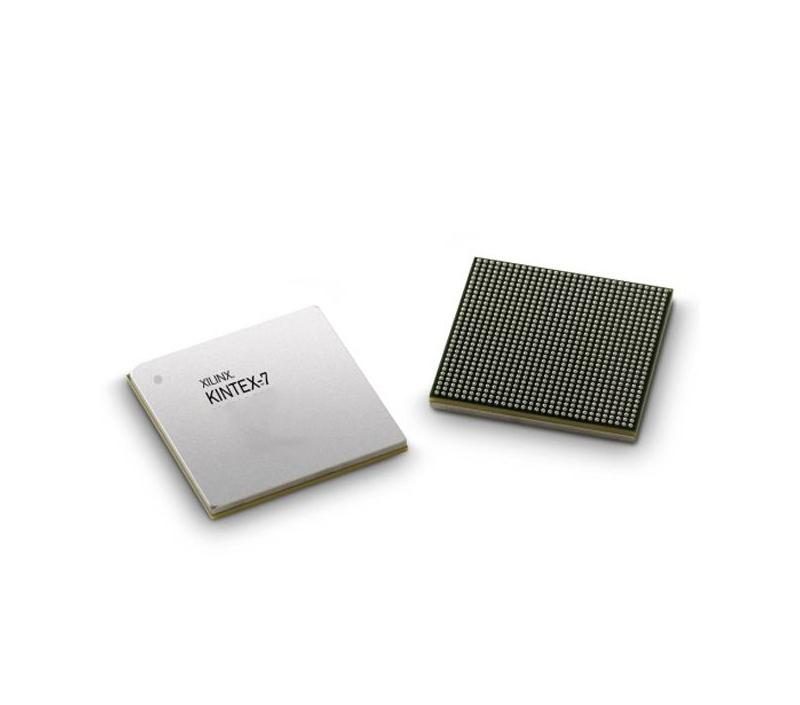
Especificaciones
Definición del número de pieza
This extended commercial temperature low-power FPGA belongs to AMD Xilinx Kintex-7 family, fabricated on mature 28nm HKMG high-k metal gate process with unified 7-series optimized architecture. It delivers balanced logic scale, DSP computing capability, high-speed serial bandwidth and power efficiency, tailored for indoor server room communication equipment, laboratory signal testing instruments, stationary industrial video processing platforms and wired transmission systems operating under stable indoor ambient temperature conditions.
- XC7K410T: Large-capacity mainstream device of Kintex-7 lineup, widely applied in medium-to-large digital signal processing, wireless communication baseband and industrial control systems, featuring outstanding cost-performance balance
- L2: Grade 2 low-power timing variant. Static and dynamic power consumption are fully optimized; thermal stability and power saving take priority over maximum operating frequency, suitable for long-term continuously running indoor devices with limited heat dissipation space
- FFG676: 676-ball compact flip-chip FCBGA package with physical dimension 27mm × 27mm. Miniaturized outline reduces overall equipment volume, while sufficient pins support full layout of all integrated GTX transceivers, general-purpose I/O circuits and multi-channel DDR3 memory interfaces with reliable signal integrity and heat dissipation performance
- E: Extended commercial temperature grade, continuous junction temperature operating range: 0°C ~ +100°C
Parámetros de los recursos de hardware integrados en el chip
1. Recursos de lógica programable
- Total System Logic Cells: 406720
- Configurable CLB Slices: 63550
- Total Flip-Flops: 1271000
- Total LUT Lookup Tables: 635500
- Distributed RAM Capacity: 5.66 Mb
2. Recursos aritméticos y de memoria integrada
- DSP48E1 arithmetic slices: 1540 units, dedicated to fixed-point/floating-point computation, large-scale FFT spectrum analysis, wireless baseband signal demodulation, radar echo processing and cryptographic algorithm acceleration tasks
- Total Block RAM Capacity: 28.62 Mb, utilized for image frame buffering, deep-depth FIFO data caching, waveform raw data storage and algorithm parameter table storage
3. Subsistema de gestión del reloj
- 10 MMCM clock management tiles
- 10 PLL phase-locked loops
Multiple mutually independent clock domains can be flexibly configured. The subsystem supports precise clock phase shifting, signal transmission delay compensation and low-jitter clock generation, fully satisfying strict synchronous timing requirements of complex communication and digital signal processing systems
4. Transceptores seriales de alta velocidad
- 16 GTX differential high-speed serial transceivers
La velocidad máxima de transmisión por carril alcanza los 12,5 Gbps, y es compatible con PCIe Gen2, 10G Ethernet, Aurora, JESD204B y los principales protocolos industriales de comunicación serie de alta velocidad. Los controladores de protocolo integrados acortan de manera efectiva el ciclo de desarrollo de las interfaces de transmisión de datos de gran ancho de banda.
5. Interfaces de E/S y módulo de monitoreo integrado en el chip
- Total configurable user I/O pins: 400
Equipped with multi-type I/O banks supporting voltage range from 1.2V to 3.3V, fully compatible with LVCMOS, LVDS, HSTL, SSTL and all conventional single-ended & differential signal standards
Embedded XADC Agile Mixed Signal monitoring module continuously collects real-time data of chip junction temperature, internal core supply voltages and external analog input signals
Características de la fuente de alimentación
The L2 low-power grade adopts reduced core operating voltage ranging from 0.97V to 1.03V. Programmable logic fabric, block RAM, DSP arrays and serial transceivers are divided into mutually independent power domains, supporting partial module power gating to dynamically reduce overall power consumption
Typical total power consumption range: 13W ~ 36W. Continuous full-load operation at the upper extended temperature limit requires forced air cooling configuration
Especificaciones de empaque y ensamblaje SMT
- Package Form: 676-pin Flip-Chip BGA
- Nivel de sensibilidad a la humedad: MSL4. Todas las operaciones de soldadura por reflujo deben completarse dentro de las 72 horas posteriores a la apertura del empaque al vacío
- Lead-free packaging design, fully compliant with RoHS3 environmental standards
- Los dispositivos se almacenan y transportan en bandejas antiestáticas para evitar daños electrostáticos durante la producción en masa de ensamblaje de placas de circuito impreso
Adaptabilidad ambiental y confiabilidad operativa
This chip is customized for indoor constant-temperature working environments. It runs stably for extended periods under mild temperature fluctuations, slight mechanical vibration and conventional electromagnetic interference. It supports AES bitstream encryption, dynamic partial reconfiguration and SEU single-event upset detection & correction, without radiation-hardened reinforcement design, and cannot adapt to outdoor low-temperature and severe rugged application scenarios
Escenarios típicos de aplicación
- Low-density 10G optical communication line cards and enterprise internal network auxiliary switching boards deployed in server rooms
- Desktop spectrum analyzers, arbitrary waveform generators and multi-channel high-speed data acquisition instruments for electronic laboratories
- Industrial 4K real-time video encoding/decoding equipment and high-precision machine vision image processing platforms
- Medium-scale communication chip prototype verification and wireless algorithm development platforms for universities and research institutes
- Indoor industrial high-speed data gateways and desktop lightweight cryptographic acceleration hardware


