






| MÃ SẢN PHẨM | BỘ PHIM | SỐ LƯỢNG PHÒNG THÍ NGHIỆM/CLBS | ĐỘ BỀN THEO TỐC ĐỘ | SỐ LƯỢNG PHẦN TỬ LỐI / TẾ BÀO | Tổng số bit RAM | SỐ LƯỢNG I/O | Điện áp – Nguồn cấp | Loại lắp đặt | NHIỆT ĐỘ HOẠT ĐỘNG | GÓI / HỘP | GÓI THIẾT BỊ CỦA NHÀ CUNG CẤP |
|---|---|---|---|---|---|---|---|---|---|---|---|
| XC7K410T-L2FFG676E | Kintex-7 | 31.775,00 | -2,00 | 406,720 | 29306880 | 400 | 0,95 ~ 1,03 V | Lắp đặt bề mặt | 0 °C ~ 100 °C | 676-BBGA, FCBGA | 676-FCBGA (27×27) |
XC7K410T-L2FFG676E
Nhà sản xuất: Xilinx
Tế bào logic: 406,720
Các lát cắt logic: 63,550
Bộ nhớ RAM tích hợp (eRAM): 28,800 Kb (800 × 36Kb Block RAM)
Dung lượng I/O tối đa của người dùng: 300
Gói: FFG676 (BGA lật chip)
Đánh giá tốc độ: -2 lít
Nhiệt độ hoạt động: Mở rộng (0°C đến +100°C)
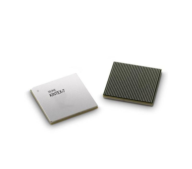
Thông số kỹ thuật
Định nghĩa mã sản phẩm
This extended commercial temperature low-power FPGA belongs to AMD Xilinx Kintex-7 family, fabricated on mature 28nm HKMG high-k metal gate process with unified 7-series optimized architecture. It delivers balanced logic scale, DSP computing capability, high-speed serial bandwidth and power efficiency, tailored for indoor server room communication equipment, laboratory signal testing instruments, stationary industrial video processing platforms and wired transmission systems operating under stable indoor ambient temperature conditions.
- XC7K410T: Large-capacity mainstream device of Kintex-7 lineup, widely applied in medium-to-large digital signal processing, wireless communication baseband and industrial control systems, featuring outstanding cost-performance balance
- L2: Grade 2 low-power timing variant. Static and dynamic power consumption are fully optimized; thermal stability and power saving take priority over maximum operating frequency, suitable for long-term continuously running indoor devices with limited heat dissipation space
- FFG676: 676-ball compact flip-chip FCBGA package with physical dimension 27mm × 27mm. Miniaturized outline reduces overall equipment volume, while sufficient pins support full layout of all integrated GTX transceivers, general-purpose I/O circuits and multi-channel DDR3 memory interfaces with reliable signal integrity and heat dissipation performance
- E: Extended commercial temperature grade, continuous junction temperature operating range: 0°C ~ +100°C
Các tham số tài nguyên phần cứng trên chip
1. Tài nguyên về logic lập trình
- Total System Logic Cells: 406720
- Configurable CLB Slices: 63550
- Total Flip-Flops: 1271000
- Total LUT Lookup Tables: 635500
- Distributed RAM Capacity: 5.66 Mb
2. Các tài nguyên toán học và bộ nhớ nhúng
- DSP48E1 arithmetic slices: 1540 units, dedicated to fixed-point/floating-point computation, large-scale FFT spectrum analysis, wireless baseband signal demodulation, radar echo processing and cryptographic algorithm acceleration tasks
- Total Block RAM Capacity: 28.62 Mb, utilized for image frame buffering, deep-depth FIFO data caching, waveform raw data storage and algorithm parameter table storage
3. Hệ thống con quản lý đồng hồ
- 10 MMCM clock management tiles
- 10 PLL phase-locked loops
Multiple mutually independent clock domains can be flexibly configured. The subsystem supports precise clock phase shifting, signal transmission delay compensation and low-jitter clock generation, fully satisfying strict synchronous timing requirements of complex communication and digital signal processing systems
4. Bộ thu phát nối tiếp tốc độ cao
- 16 GTX differential high-speed serial transceivers
Tốc độ truyền dẫn tối đa trên mỗi làn đạt 12,5 Gbps, tương thích với các giao thức truyền thông nối tiếp tốc độ cao công nghiệp phổ biến như PCIe Gen2, 10G Ethernet, Aurora và JESD204B. Các bộ điều khiển giao thức cứng tích hợp giúp rút ngắn hiệu quả chu kỳ phát triển của các giao diện truyền dữ liệu băng thông rộng.
5. Giao diện I/O và mô-đun giám sát trên chip
- Total configurable user I/O pins: 400
Equipped with multi-type I/O banks supporting voltage range from 1.2V to 3.3V, fully compatible with LVCMOS, LVDS, HSTL, SSTL and all conventional single-ended & differential signal standards
Embedded XADC Agile Mixed Signal monitoring module continuously collects real-time data of chip junction temperature, internal core supply voltages and external analog input signals
Đặc tính của bộ nguồn
The L2 low-power grade adopts reduced core operating voltage ranging from 0.97V to 1.03V. Programmable logic fabric, block RAM, DSP arrays and serial transceivers are divided into mutually independent power domains, supporting partial module power gating to dynamically reduce overall power consumption
Typical total power consumption range: 13W ~ 36W. Continuous full-load operation at the upper extended temperature limit requires forced air cooling configuration
Thông số kỹ thuật về đóng gói và lắp ráp SMT
- Package Form: 676-pin Flip-Chip BGA
- Mức độ nhạy cảm với độ ẩm: MSL4. Tất cả các công đoạn hàn nóng chảy phải được hoàn thành trong vòng 72 giờ sau khi mở bao bì chân không
- Lead-free packaging design, fully compliant with RoHS3 environmental standards
- Các thiết bị được bảo quản và vận chuyển trong các khay chống tĩnh điện để tránh hư hỏng do tĩnh điện trong quá trình sản xuất hàng loạt bảng mạch in (PCB)
Khả năng thích ứng với môi trường và độ tin cậy trong vận hành
This chip is customized for indoor constant-temperature working environments. It runs stably for extended periods under mild temperature fluctuations, slight mechanical vibration and conventional electromagnetic interference. It supports AES bitstream encryption, dynamic partial reconfiguration and SEU single-event upset detection & correction, without radiation-hardened reinforcement design, and cannot adapt to outdoor low-temperature and severe rugged application scenarios
Các tình huống ứng dụng điển hình
- Low-density 10G optical communication line cards and enterprise internal network auxiliary switching boards deployed in server rooms
- Desktop spectrum analyzers, arbitrary waveform generators and multi-channel high-speed data acquisition instruments for electronic laboratories
- Industrial 4K real-time video encoding/decoding equipment and high-precision machine vision image processing platforms
- Medium-scale communication chip prototype verification and wireless algorithm development platforms for universities and research institutes
- Indoor industrial high-speed data gateways and desktop lightweight cryptographic acceleration hardware


