






XC7A200T-2FFG1156E
Fabricante: Xilinx
Células lógicas: 215,360
Rebanadas lógicas: 33,650
RAM integrada (eRAM): 13 140 Kb (365 bloques de RAM de 36 Kb)
E/S máxima por usuario: 500
Paquete: FFG1156 (BGA con chip invertido)
Grado de velocidad: -2
Temperatura de funcionamiento: Ampliado (0 °C a +100 °C)
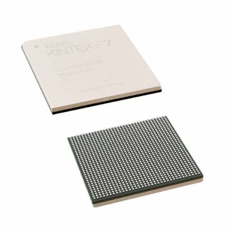
Especificaciones
Definición del número de pieza
This is a high-density extended industrial temperature FPGA belonging to Xilinx Artix-7 series, manufactured via mature 28nm low-power semiconductor process. It balances ample computing resources, flexible I/O scalability and favorable cost, designed for complex embedded vision, multi-channel data acquisition and industrial communication devices requiring wide-temperature stable operation and abundant peripheral expansion interfaces.
- XC7A200T: Top high-density model of Artix-7 FPGA family
- -2: Speed Grade 2, universal balanced timing grade. It reserves sufficient timing margin for most medium-to-large scale digital designs, realizing an optimal trade-off between operating frequency, timing closure stability and total power consumption
- FFG1156: 1156-ball flip-chip FCBGA large-size package. Massive pin resources support extensive parallel signal access, multi-peripheral docking and full utilization of on-chip high-speed transceivers
- E: Extended industrial temperature rating, operating junction temperature range: -40°C ~ +100°C
On-Chip Hardware Resource Specifications
1. Recursos generales sobre lógica programable
- Total Logic Cells: 215,360
- Configurable Slices: 33,650
- Total Flip-Flops: 269,200
- Total LUTs: 134,600
2. Recursos aritméticos y de memoria integrada
- DSP48E1 arithmetic slices: 740 units, applicable to FFT signal calculation, digital filtering, real-time image pixel processing, multi-axis motor control algorithms and medium-scale matrix operation acceleration
- Total Block RAM Capacity: 13,140 Kb, used for high-capacity image frame caching, deep FIFO data buffering, waveform storage and algorithm parameter lookup tables
- Distributed RAM Capacity: 3,888 Kb
3. Subsistema de gestión del reloj
- 8 bloques de gestión de reloj MMCM
- 8 PLL phase locked loops
Supports multi-clock domain generation, clock phase fine adjustment, delay compensation and high-frequency jitter suppression, meeting strict synchronous timing requirements of complex embedded digital systems
4. Transceptores seriales de alta velocidad
- 8 GTX high-speed differential transceivers
Maximum line rate up to 6.6 Gbps, compatible with PCIe Gen2, Gigabit Ethernet, Aurora, CPRI and other mainstream serial communication protocols
5. Interfaces de E/S y módulo de monitoreo integrado en el chip
- Pines de E/S configurables para el usuario: 560
Voltaje del banco de E/S ajustable de 1,2 V a 3,3 V, totalmente compatible con LVCMOS, LVDS, HSTL, SSTL y todos los estándares de señal diferencial más comunes
Integrated dual-channel 12-bit XADC analog monitor, which continuously monitors die junction temperature, all internal power supply voltages and external analog input signals in real time
Especificaciones de la fuente de alimentación
Nominal core internal operating voltage: 1.0V
Independent isolated power domains are configured for logic fabric, Block RAM, DSP array and high-speed transceivers separately
Typical overall power consumption: 4.5W ~ 18W; passive heat dissipation satisfies conventional continuous operation requirements under most industrial working conditions, while active cooling is recommended under full-load high-temperature operation
Requisitos de empaque y ensamblaje SMT
- Tipo de paquete: FCBGA (matriz de bolas) de 1156 pines con tecnología flip-chip
- Nivel de sensibilidad a la humedad: MSL4; todos los procesos de soldadura por reflujo deben completarse en un plazo de 72 horas después de abrir el empaque al vacío
- Fabricación sin plomo, que cumple plenamente con las directivas ambientales de la RoHS
- Se entregan y almacenan en bandejas antiestáticas para evitar daños electrostáticos durante la producción automatizada en masa de placas de circuito impreso
Adaptabilidad ambiental y confiabilidad
The chip maintains stable long-term operation under drastic temperature fluctuations, mechanical vibration, shock and moderate electromagnetic interference harsh industrial environments. It supports AES bitstream encryption protection and SEU single-event upset error detection, featuring excellent cost performance and field anti-interference capability.
Escenarios típicos de aplicación
- Multi-channel high-precision motion control hosts, large-scale industrial automation main control units
- Multi-port industrial Ethernet convergence gateways, cross-protocol field bus switching equipment
- Multi-channel high-speed signal acquisition analyzers, comprehensive on-site environmental monitoring systems
- Multi-camera industrial machine vision inspection main control boards, real-time image processing platforms
- Medical imaging auxiliary data processing and control modules
- Wide-temperature industrial high-performance SOM core boards and embedded complex algorithm verification platforms


