






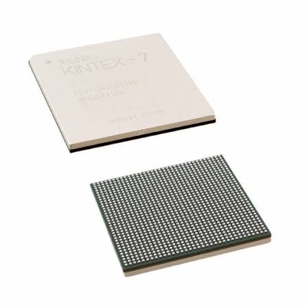
XC7A200T-2FFG1156E
Производитель: Xilinx
Логические ячейки: 215,360
Логические срезы: 33,650
Встроенная оперативная память (eRAM): 13 140 Кб (365 × 36 Кб блочной оперативной памяти)
Максимальный пользовательский ввод/вывод: 500
Упаковка: FFG1156 (Flip-Chip BGA)
Класс скорости: -2
Рабочая температура: Расширенный (от 0°C до +100°C)
Технические характеристики
Определение номера детали
This is a high-density extended industrial temperature FPGA belonging to Xilinx Artix-7 series, manufactured via mature 28nm low-power semiconductor process. It balances ample computing resources, flexible I/O scalability and favorable cost, designed for complex embedded vision, multi-channel data acquisition and industrial communication devices requiring wide-temperature stable operation and abundant peripheral expansion interfaces.
- XC7A200T: Top high-density model of Artix-7 FPGA family
- -2: Speed Grade 2, universal balanced timing grade. It reserves sufficient timing margin for most medium-to-large scale digital designs, realizing an optimal trade-off between operating frequency, timing closure stability and total power consumption
- FFG1156: 1156-ball flip-chip FCBGA large-size package. Massive pin resources support extensive parallel signal access, multi-peripheral docking and full utilization of on-chip high-speed transceivers
- E: Extended industrial temperature rating, operating junction temperature range: -40°C ~ +100°C
On-Chip Hardware Resource Specifications
1. General Programmable Logic Resources
- Total Logic Cells: 215,360
- Configurable Slices: 33,650
- Total Flip-Flops: 269,200
- Total LUTs: 134,600
2. Арифметические ресурсы и встроенная память
- DSP48E1 arithmetic slices: 740 units, applicable to FFT signal calculation, digital filtering, real-time image pixel processing, multi-axis motor control algorithms and medium-scale matrix operation acceleration
- Total Block RAM Capacity: 13,140 Kb, used for high-capacity image frame caching, deep FIFO data buffering, waveform storage and algorithm parameter lookup tables
- Distributed RAM Capacity: 3,888 Kb
3. Подсистема управления часами
- 8 MMCM clock management tiles
- 8 PLL phase locked loops
Supports multi-clock domain generation, clock phase fine adjustment, delay compensation and high-frequency jitter suppression, meeting strict synchronous timing requirements of complex embedded digital systems
4. Высокоскоростные последовательные приемопередатчики
- 8 GTX high-speed differential transceivers
Maximum line rate up to 6.6 Gbps, compatible with PCIe Gen2, Gigabit Ethernet, Aurora, CPRI and other mainstream serial communication protocols
5. I/O Interfaces & On-Chip Monitoring Module
- Configurable user I/O pins: 560
I/O bank voltage adjustable from 1.2V to 3.3V, fully compatible with LVCMOS, LVDS, HSTL, SSTL and all mainstream differential signal standards
Integrated dual-channel 12-bit XADC analog monitor, which continuously monitors die junction temperature, all internal power supply voltages and external analog input signals in real time
Технические характеристики источника питания
Nominal core internal operating voltage: 1.0V
Independent isolated power domains are configured for logic fabric, Block RAM, DSP array and high-speed transceivers separately
Typical overall power consumption: 4.5W ~ 18W; passive heat dissipation satisfies conventional continuous operation requirements under most industrial working conditions, while active cooling is recommended under full-load high-temperature operation
Packaging & SMT Assembly Requirements
- Package Type: 1156-pin flip-chip FCBGA ball grid array
- Moisture Sensitivity Level: MSL4; all reflow soldering processes must be completed within 72 hours after vacuum packaging is opened
- Lead-free construction, fully compliant with RoHS environmental directives
- Delivered and stored in anti-static trays to prevent electrostatic damage during automated PCB mass production
Environmental Adaptability & Reliability
The chip maintains stable long-term operation under drastic temperature fluctuations, mechanical vibration, shock and moderate electromagnetic interference harsh industrial environments. It supports AES bitstream encryption protection and SEU single-event upset error detection, featuring excellent cost performance and field anti-interference capability.
Типичные сценарии применения
- Multi-channel high-precision motion control hosts, large-scale industrial automation main control units
- Multi-port industrial Ethernet convergence gateways, cross-protocol field bus switching equipment
- Multi-channel high-speed signal acquisition analyzers, comprehensive on-site environmental monitoring systems
- Multi-camera industrial machine vision inspection main control boards, real-time image processing platforms
- Medical imaging auxiliary data processing and control modules
- Wide-temperature industrial high-performance SOM core boards and embedded complex algorithm verification platforms


