






XC6VLX240T-L1FFG784C
Hersteller: Xilinx
Logische Zellen: 241,152
Logische Schnitte: 37,680
Eingebettetes RAM (eRAM): 14.976 Kb (832 × 18 Kb Block-RAM)
Maximale Benutzer-E/A: 360
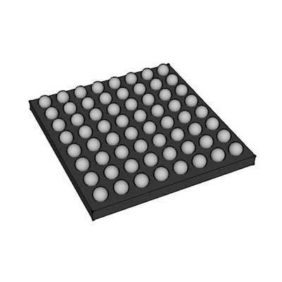
Paket: FFG784 (Flip-Chip BGA)
Geschwindigkeitsstufe: -1L
Betriebstemperatur: Handelsüblich (0°C bis +85°C)
Spezifikationen
Part Number Detailed Explanation
This is a low-power optimized commercial temperature FPGA from Xilinx Virtex-6 LXT series, manufactured on 40nm semiconductor process. It combines moderate-scale logic resources, built-in high-speed serial transceivers and low-power silicon tuning, designed for power-sensitive embedded systems, communication intermediate equipment and desktop signal processing devices running under stable indoor ambient conditions.
- XC6VLX240T: Mid-large density chip of Virtex-6 LXT family; LXT indicates the variant equipped with GTX high-speed serial transceivers
- L1: Low-power optimized speed grade 1. It features lowered static power consumption and relaxed timing parameters for power saving, prioritizing low energy draw over maximum operating frequency
- FFG784: 784-ball flip-chip FCBGA package, moderate overall size balancing layout space and available I/O resources
- C: Commercial temperature grade, operating junction temperature range: 0°C ~ +85°C
On-Chip Hardware Resource Allocation
1. General Programmable Logic Resources
- Total Logic Cells: 241,152
- Configurable Slices: 37,680
- Total Flip-Flops: 301,440
- Total LUTs: 150,720
2. Arithmetic and Embedded Memory Resources
- DSP48E1 arithmetic units: 1,064 pieces, suitable for digital filtering, FFT signal processing, communication baseband algorithms, image processing and medium-scale matrix calculations
- Total Block RAM capacity: 15,408 Kb, used for data FIFO buffering, waveform storage, image frame caching and algorithm parameter lookup tables
- Distributed RAM capacity: 5,328 Kb
3. Clock Management Subsystem
- 12 MMCM clock management tiles
- 12 PLL phase locked loops
Supports multi-clock domain generation, phase shifting, clock delay compensation and high-frequency jitter suppression, meeting timing demands of complex multi-module digital systems
4. Serielle Hochgeschwindigkeits-Transceiver
- 12 GTX high-speed differential transceivers
Maximum transmission rate up to 6.6 Gbps, compatible with PCIe Gen2, Aurora, CPRI, Gigabit Ethernet and other mainstream serial communication protocols
Hard PCIe 2.0 IP core is embedded for rapid PCIe interface development
5. I/O Interfaces & On-Chip Monitoring Module
- Configurable user I/O pins: 448
I/O bank voltage configurable from 1.2V to 3.3V, fully supports LVCMOS, LVDS, HSTL, SSTL and common differential signal standards
Built-in dual-channel 12-bit System Monitor XADC module, real-time monitoring of chip junction temperature, internal power supply voltages and external analog input signals
Technische Daten zum Netzteil
Nominal core operating voltage: 1.0V with low-power tuning
Logic fabric, block RAM, DSP arrays and serial transceivers adopt independent isolated power domains
Typical overall power consumption: 7W ~ 21W; passive heat dissipation can satisfy continuous stable operation under conventional indoor working loads
Packaging & SMT Assembly Standards
- Package Type: 784-pin flip-chip FCBGA ball grid array
- Feuchtigkeitsempfindlichkeitsstufe: MSL4; alle Reflow-Lötprozesse müssen innerhalb von 72 Stunden nach dem Öffnen der Vakuumverpackung abgeschlossen sein
- Lead-free packaging design, fully compliant with RoHS environmental regulations
- Packed and delivered in anti-static trays to avoid electrostatic damage during automated PCB mass production
Umweltverträglichkeit und Zuverlässigkeit
This chip is tailored for constant-temperature indoor environments such as laboratories and equipment rooms. It supports bitstream encryption and SEU error detection, delivering stable operation for communication equipment, prototype verification platforms and indoor signal processing devices without extreme temperature fluctuation interference.
Typische Anwendungsszenarien
- Communication access network intermediate processing boards, wired transmission protocol conversion equipment
- Laboratory signal acquisition and analysis instruments, desktop waveform generators
- Early-stage digital chip prototype verification platforms, algorithm development test boards
- Multi-channel audio and video real-time processing equipment, broadcasting signal modulation modules
- Industrial indoor testing main control boards, non-rugged embedded computing units
- Low-power development platforms for communication algorithm research


