






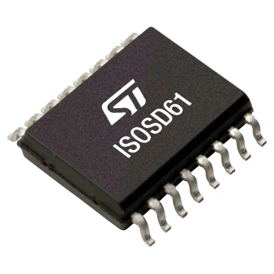
Spezifikationen
Hersteller: STMicroelectronics
Device Type: Galvanically isolated second-order sigma-delta modulator, tape and reel surface mount packaged precision analog signal conversion IC designed for isolated current and voltage sampling in industrial power conversion systems
Elektrische Daten
Dual-side supply voltage range: 3.0 V to 5.5 V
Maximum external synchronous input clock frequency: 25 MHz
Full-scale differential analog input range: ±320 mV
Conversion performance parameters
Nominal resolution: 16-bit with no missing codes
Typical effective number of bits: 13 bits
Typical signal-to-noise ratio: 86 dB
Typical total harmonic distortion: -83 dB
Maximum gain error: 1%
Typical integral non-linearity: ±3 LSB
Isolation and anti-interference indicators
Peak isolation withstand voltage: 6000 V
Continuous working isolation voltage: 1200 V peak
Common-mode transient immunity: 30 kV/μs
Digital output interface options: single-ended TTL/CMOS level
Operating temperature scope: -40°C to +125°C
Package specification: 16-pin wide-body SOIC surface mount housing
Wesentliche funktionale Merkmale
The chip adopts built-in micro-transformer isolation architecture to realize complete electrical separation between the analog sampling side and digital host communication side, which avoids the aging and performance attenuation defects of traditional optocoupler isolation schemes, featuring longer service life, faster transmission speed and lower power consumption.
It converts low-amplitude differential analog voltage signals into high-speed 1-bit serial digital bitstream output. The original analog waveform can be accurately restored after digital filtering and decimation processing through FPGA or main control microcontroller, and third-order SINC filter is the most matched decoding scheme.
Two optional digital output modes are reserved for flexible system layout deployment. This model supports single-ended TTL/CMOS electrical level, and another derivative version supports LVDS differential signal transmission for stronger electromagnetic interference suppression under high noise conditions.
Excellent common-mode noise suppression capability adapts to high voltage and high transient interference working environments. It can effectively isolate the high common-mode voltage difference between power primary side and control secondary side, ensuring sampling precision will not be affected by power fluctuation and switching noise.
Wide industrial temperature working range keeps consistent conversion accuracy under extreme cold and high-temperature working conditions. All internal circuits are optimized for industrial harsh environments with complete electrostatic protection on each pin.
The synchronous external clock design facilitates multi-channel sampling signal alignment in multi-loop power control systems, simplifying system timing synchronization development work.
Typische Anwendungsszenarien
Industrial servo motor and frequency converter current closed-loop sampling
Solar photovoltaic inverter DC bus voltage and inverter arm current detection
Uninterruptible power supply and high-power switching power supply isolated sampling
Electric vehicle on-board charger power loop current monitoring
Server and communication equipment high-efficiency power module signal acquisition
Factory automation high-voltage equipment analog signal isolated transmission


