





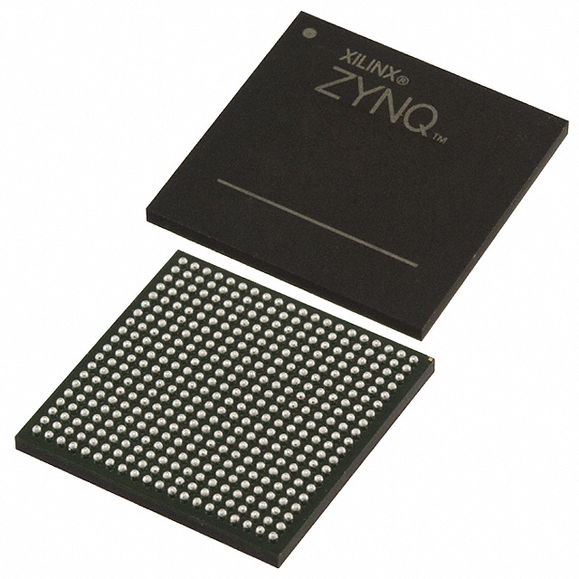
XC7Z010-2CLG400I
Manufacturer: AMD (Xilinx)
Logic Cells: 28,000
Logic Slices: 4,400
Embedded RAM (eRAM): 2,160 Kb (120 × 18Kb Block RAM)
Package: CLG400 (CSBGA-400)
Operating Temperature: Industrial (-40°C to +100°C)
Specifications
Part Number Definition
This is Xilinx Zynq-7000 series all-programmable heterogeneous SoC based on 28nm manufacturing process, integrating dual-core ARM Cortex-A9 processor subsystem and Artix-7 programmable logic resources, oriented to low-cost small-scale embedded control and lightweight data processing scenarios.
- XC7Z010: Entry-level chip of Zynq-7000 family
- -2: Speed Grade 2, high timing performance grade with sufficient margin for stable high-speed circuit design
- CLG400: 400-ball compact CSPBGA packaging
- I: Industrial temperature grade, junction temperature operating range: -40°C ~ +100°C
Complete On-Chip Hardware Architecture
1. Processing System (PS: ARM Processor Domain)
- Dual-core ARM Cortex-A9 processors, maximum operating frequency up to 766 MHz
- Each core owns independent 32KB instruction cache and 32KB data cache; 256KB shared L2 cache
- Built-in NEON SIMD floating-point acceleration unit for audio, image and simple signal arithmetic operations
- Rich peripheral controllers: Dual Gigabit Ethernet, USB 2.0 OTG, SD card interface, CAN bus, UART, SPI, I2C, general GPIO
- Supports secure boot mechanism to protect system startup security
2. Programmable Logic Fabric (PL: FPGA Part)
FPGA architecture consistent with Artix-7 series
- Total Logic Cells: 28800
- Configurable Logic Slices: 4500
- DSP48E1 arithmetic blocks: 80 units, used for simple filtering, FFT calculation, sensor data acquisition and low-speed algorithm acceleration
- Total Block RAM capacity: 2.16 Mbit
- Integrated MMCM and PLL clock management modules to generate multi-group clocks and suppress clock jitter
- No on-chip high-speed serial transceivers
3. I/O Resources & Analog Monitoring Module
- Available user general I/O pins: 156
- I/O banks support configurable voltage of 1.2V / 1.5V / 1.8V / 2.5V / 3.3V, compatible with LVCMOS, LVDS differential signaling standards
- On-chip dual-channel 12-bit XADC monitor: real-time detection of die temperature, internal power supply voltages and external analog input signals
Power Supply Parameters
Separate power domains are allocated for processor system and programmable logic. Nominal core voltage is 1.0 V.
Typical overall power consumption ranges from 2.5 W to 12 W, passive heat dissipation is applicable for compact embedded devices.
Packaging and Assembly Specifications
- Package: 400-pin CSPBGA ball grid array
- Moisture Sensitivity Level: MSL3; reflow soldering must be finished within 168 hours after vacuum packaging is opened
- Lead-free packaging, fully compliant with RoHS environmental standards
- Shipped in anti-static trays for automated industrial PCB mass production
Environmental and Reliability Characteristics
Stable long-term operation under drastic temperature fluctuation and strong electromagnetic interference conditions.
Equipped with bitstream encryption protection and SEU error checking function, meeting reliability requirements of industrial control, vehicle-mounted terminals and outdoor IoT equipment.
Typical Application Fields
- Small industrial controllers, low-end PLC, servo auxiliary control boards and field bus protocol converters
- Miniature IoT gateway, remote data collection terminal and environmental monitoring node
- Portable data loggers, vibration acquisition equipment and simple handheld measuring instruments
- Tiny embedded vision devices: image snapshot, video streaming transmission and basic image preprocessing
- Household medical portable detection equipment main control modules
- Low-cost secondary development core boards and serial port expansion control boards


