





| Mfr Part | Series | Manufacturer | Package | Topology | Product Status | Mounting Type | Switching Frequency | Function | Input Voltage | Output Voltage | Number of Outputs | Operating Temperature | Output Type | Output Current |
|---|---|---|---|---|---|---|---|---|---|---|---|---|---|---|
| HMC7044LP10BETR | Clock Gen | Analog Devices | LFCSP-56 | PLL | Active | Surface Mount | N/A | Jitter Cleaner | 3.3 V | Clock | 14 | -40°C to +85°C | LVDS/CMOS | N/A |
HMC7044LP10BETR
Manufacturer: Analog Devices
Logic Cells: Clock generation and jitter cleaner IC
Logic Slices: PLL, VCO control, clock distribution logic
Embedded RAM (eRAM): Internal configuration registers
Package: LFCSP-64
Operating Temperature: -40 °C to +85 °C
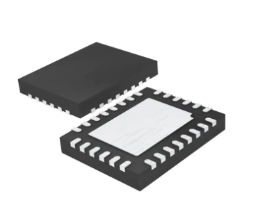
Specifications
This is a high-performance dual-loop integer-N jitter attenuator and multi-channel clock management IC developed by Analog Devices, tailored for ultra-low phase noise clock generation and distribution in high-speed communication and RF systems, fully compliant with JESD204B and JESD204C high-speed serial interface standards.
Part Number Definition
HMC7044 refers to the core model of wideband low-jitter clock attenuator series. LP10 stands for 68-lead 10mm×10mm exposed pad LFCSP surface mount package. BE denotes industrial-grade complete configuration version. TR means tape-and-reel continuous reel packaging for automated SMT mass production mounting.
Core Electrical Performance Parameters
The chip adopts dual independent PLL architecture paired with dual narrowband on-chip VCO cores, covering mainstream RF clock frequency bands around 2.5GHz and 3GHz. The maximum clock output frequency reaches 3.2GHz, delivering ultra-low timing jitter performance with typical RMS jitter as low as 44fs within 12kHz~20MHz integration bandwidth. Its phase noise floor can reach -156dBc/Hz, and low offset phase noise ensures clean clock signals for high-speed data converters.
A total of 14 configurable differential clock output channels are integrated, supporting LVDS, LVPECL, CML multiple electrical signaling standards. Each channel is independently programmable with 25ps analog fine delay and half VCO cycle digital coarse delay, facilitating precise clock alignment and synchronization across multi-device boards.
It accepts up to 4 reference clock inputs with multiple level compatibility, built-in signal loss detection and hitless reference switching function; frequency holdover mode maintains stable output frequency temporarily after reference signal interruption. System working parameters, power consumption and phase noise trade-off settings are fully configurable via SPI bus. On-chip linear regulators provide excellent power supply rejection capability to resist board power fluctuation interference.
Dual power supply design with main supply voltage ranging from 3.135V to 3.465V, matched with internal core low-voltage power rail to balance noise performance and overall power consumption. Reserved SYSREF synchronization signal output and interrupt pins greatly simplify the synchronization workflow of JESD204 serial links.
Packaging and Assembly Specifications
68-pin LFCSP-VQ leadless exposed pad package with overall dimension 10mm×10mm. The bottom large-area metal pad efficiently dissipates heat generated during continuous full-channel operation and stabilizes internal circuit temperature. It is classified as MSL3 moisture sensitive component, all reflow soldering procedures need to be finished within 168 hours after unpacking original vacuum packaging. Standard reel feeding packaging is adopted to match fully automatic placement equipment on production lines.
Environmental and Compliance Standards
Stable continuous operating temperature range covers -40℃ ~ +85℃, suitable for communication equipment cabinets, microwave radio units and industrial test instruments with large ambient temperature variation. The whole device is produced with lead-free manufacturing process and complies with global environmental material control regulations. Highly integrated clock tree function replaces discrete PLL and clock buffer chips, effectively reducing peripheral component count and PCB layout complexity.
Typical Application Fields
4G/5G cellular base station radio unit and baseband board clock distribution system
High-speed ADC/DAC converter reference clock generation for radar and microwave imaging equipment
Phased array antenna timing reference network and broadband wireless access equipment
High-precision signal analyzers, spectrum analyzers and other RF automatic test equipment
High-speed data acquisition boards, FPGA-based high-speed link synchronization timing modules
LXB Semicon supplies original Analog Devices HMC7044LP10BETR multi-output ultra-low jitter clock attenuator IC


