





| Mfr Part | Series | Manufacturer | Package | Topology | Product Status | Mounting Type | Switching Frequency | Function | Input Voltage | Output Voltage | Number of Outputs | Operating Temperature | Output Type | Output Current |
|---|---|---|---|---|---|---|---|---|---|---|---|---|---|---|
| HMC252AQS24E | RF Switch | Analog Devices | QSOP-24 | N/A | Active | Surface Mount | N/A | RF Switch | ±5 V | RF | 1 | -40°C to +85°C | RF | N/A |
HMC252AQS24E
Manufacturer: Analog Devices
Logic Cells: RF amplifier
Logic Slices: Wideband gain amplification circuitry
Embedded RAM (eRAM): –
Package: QSOP-24
Operating Temperature: -40 °C to +85 °C
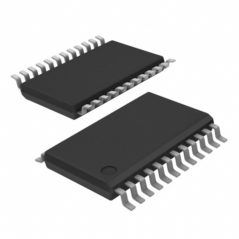
Specifications
This is a broadband non-reflective SP6T RF switch fabricated with GaAs MMIC process by Analog Devices, designed for multi-channel radio frequency signal routing selection within DC~3GHz frequency band, integrating built-in decoding logic circuit to simplify external control circuit design.
Part Number Definition
HMC252A stands for the core model of six-channel single-pole multi-throw RF switch series. QS24 refers to 24-pin QSOP surface mount package. E represents industrial grade complete functional version compliant with lead-free environmental standards.
Core Electrical Performance Parameters
The effective working frequency range covers direct current up to 3GHz, matched with standard 50Ω RF system impedance. It features ultra-low insertion loss, only 1.0dB at 2GHz working frequency; channel isolation performance is excellent, reaching 45dB at low frequency band and maintaining 26dB isolation at the upper limit 3GHz, effectively avoiding signal crosstalk between different channels.
The chip is internally integrated with 3-to-6 TTL hardware decoder, only three digital control pins are required to complete switching selection of six signal channels, no external logic gate chips need to be matched. It adopts single positive power supply design, applicable voltage range 3V~5V, fully compatible with TTL and CMOS logic level drive, quiescent operating current is kept at 8mA with low power consumption.
1dB compression output power reaches 28dBm, strong signal bearing capacity; all idle channels maintain 50Ω impedance matching state all the time, belonging to non-reflective switch structure, which can avoid standing wave fluctuation and signal distortion during channel switching.
Packaging and Assembly Specifications
Adopts 24-pin narrow-body QSOP patch package, compact overall size suitable for miniaturized RF board layout. It is classified as MSL3 moisture sensitive component, reflow soldering operation must be finished within 168 hours after opening original vacuum packaging. Tape-and-reel reel packaging is provided to adapt to automatic SMT placement on mass production lines.
Environmental and Compliance Standards
Continuous stable operating temperature range is -40℃ ~ +85℃, adapting to communication base station equipment, indoor wireless equipment and precision testing instruments with variable temperature environment. The whole product is manufactured with lead-free process and complies with universal environmental restriction specifications. Highly integrated structure can replace multiple discrete single-pole double-throw switches and peripheral drive circuits, greatly reducing the number of peripheral components and PCB layout difficulty.
Typical Application Fields
Wireless communication base station front-end signal channel switching and antenna selection circuit
CATV cable television receiving equipment, satellite signal receiving terminal signal gating unit
Wireless LAN module, broadband access equipment multi-frequency signal selection circuit
Spectrum analyzer, signal generator and other precision RF test instrument channel switching module
Microwave remote sensing equipment, short-distance radio transmission equipment multi-path signal distribution system
LXB Semicon supplies original Analog Devices HMC252AQS24E six-channel broadband RF switching integrated circuit


