





| Mfr Part | Manufacturer | FPGA Family | Logic Elements (LEs) | Embedded Memory | DSP / Multipliers | Max I/O Count | Core Voltage | I/O Voltage | Operating Temperature | Package | Process Node | Typical Max Frequency | Target Applications | RoHS |
| EP4CE10E22C8N | ALTERA | Cyclone® IV E | 10320 | ~414 Kbits | 46 × 18×18 | Package dependent | 1.15–1.25 V | Up to 3.3 V | −40 °C to +85 °C | FBGA | 60 nm | ~200 MHz | Embedded control, automation | Yes |
EP4CE10E22C8N
Manufacturer: Altera (Intel)
Logic Cells: 10,320 Logic Elements (LEs)
Logic Slices: Logic Array Blocks (LABs)
Embedded RAM (eRAM): 414 Kbits embedded memory
Package: EQFP-144
Operating Temperature: Commercial (0 °C to +85 °C)
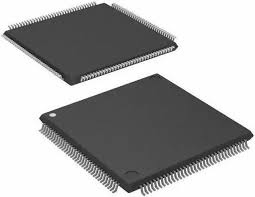
Specifications
EP4CE10E22C8N is an Intel (Altera) Cyclone IV E low-cost, low-power commercial FPGA built on optimized 60nm process, designed for mid-low complexity digital logic, peripheral bridging and lightweight signal processing with excellent cost-performance balance for mass-volume equipment projects.
👉 It’s not a high-density high-speed FPGA with built-in high-speed serial transceivers.
👉 It’s an economical general-purpose programmable logic chip targeting cost-sensitive industrial control, educational development boards and consumer embedded hardware.
Key Features of EP4CE10E22C8N Cyclone IV E FPGA
Digital hardware designers and equipment manufacturers select EP4CE10E22C8N for its sufficient logic resources, compact flat-pack packaging and ultra-low static power consumption:
- Equipped with 10,320 logic elements (LEs) to implement medium-scale parallel digital logic and state machine designs
- Total 414 Kbit on-chip embedded block RAM for FIFO cache, data buffering and lookup table storage
- Multiple built-in 18×18-bit hardware multipliers for lightweight DSP algorithms, PID motion control and simple filter calculation
- Dual independent PLL clock modules, supporting maximum internal operating frequency up to 402 MHz for multi-clock domain design
- -8 commercial speed grade for stable timing closure under mainstream working frequency scenarios
- 144-pin EQFP (TQFP) surface mount package, bringing out 91 configurable user I/O pins for multi-peripheral connection
- Core supply voltage range: 1.15 V ~ 1.25 V; I/O banks support 1.2 V / 1.5 V / 1.8 V / 2.5 V / 3.3 V LVTTL/LVCMOS standards
- Multiple configuration modes supported: JTAG, Active Serial (AS), Passive Serial for flexible firmware download and online debugging
- Native compatible with Nios II soft-core processor to build small single-chip embedded SoC without extra CPU chips
- Ultra-low power architecture; total power consumption less than 1.5 W for most protocol bridging applications
- Commercial operating temperature range: 0°C to +85°C junction temperature
- MSL 3 moisture sensitivity rating, RoHS-compliant lead-free packaging compatible with standard SMT mass production lines
- Stable long-lifecycle component supply for legacy equipment maintenance and small-batch industrial upgrade projects
Typical applications
Entry-level FPGA teaching development boards and university electronic experiment platforms
Small industrial PLC auxiliary logic and multi-channel sensor signal acquisition modules
Low-speed communication protocol conversion boards and serial bus signal bridge hardware
Stepper & BLDC motor single/multi-axis motion control drive logic circuits
Audio signal filtering, simple image pre-processing and low-rate data processing units
Portable test & measurement instruments, signal generators and timing control boards
LED screen display driver, digital pulse generation and switching signal conditioning hardware
Smart home control peripheral expansion and industrial IoT edge logic processing terminals
Medical portable testing equipment digital control subsystems
Cost-sensitive consumer electronic interface expansion and logic replacement for traditional CPLD
LXB Semicon supplies original EP4CE10E22C8N FPGA


