





| MODEL P/N | SERIES | NUMBER OF LABS/CLBS | SPEED GRADE | NUMBER OF LOGIC ELEMENTS / CELLS | TOTAL RAM BITS | NUMBER OF I/O | VOLTAGE – SUPPLY | MOUNTING TYPE | OPERATING TEMPERATURE | PACKAGE / CASE | SUPPLIER DEVICE PACKAGE |
|---|---|---|---|---|---|---|---|---|---|---|---|
| ADSP-TS201SABPZ-050 | TigerSHARC (ADSP-TS201S) | 0,00 | 500,00 | N/A | 24 Mbit on-chip DRAM | 576 | VDD = 1.05 V (core) / VDD_IO = 2.50 V / VDD_DRAM = 1.5 V. | Surface mount (BGA) | −40 °C to +85 °C (TC) | 576-BBGA (BP-576) | 576-BGA-ED (25×25) |
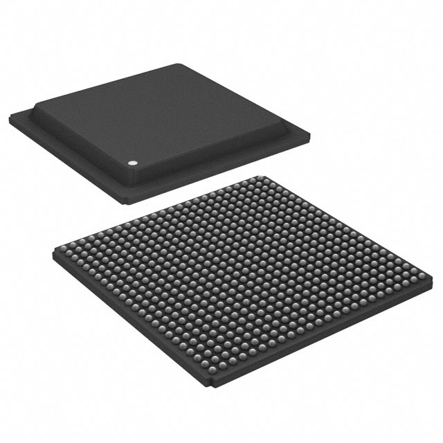
ADSP-TS201SABPZ-050
Manufacturer: Analog Devices
Logic Cells: бк
Logic Slices: бк
Embedded RAM (eRAM): 24 Mbits On-Chip SRAM
Package: SABP
Operating Temperature: ?40°C to +85°C
Specifications
Part Number Definition
ADSP-TS201S belongs to Analog Devices TigerSHARC series high-performance floating-point digital signal processor, oriented to intensive real-time signal processing and multi-processor parallel array construction.
Suffix code interpretation:
AB: Industrial temperature range rating
BP: Thermally enhanced 576-ball BGA package with overall dimension 25mm × 25mm
Z: Lead-free construction, compliant with RoHS requirements
-050: Rated core operating frequency of 500 MHz
The device is packed in anti-static trays for automated SMT assembly, and this product generation has been officially discontinued.
Core Electrical Performance Parameters
Processor Computing Core
The chip adopts static superscalar VLIW architecture with two parallel arithmetic execution units and SIMD parallel operation capability. Each computing unit is equipped with arithmetic logic unit, dedicated hardware multiplier and barrel shifter. Dual independent address generators are integrated to accelerate circular addressing and bit-reversal addressing essential for FFT algorithms.
Supported data formats include 8/16/32/64-bit fixed-point values, 32-bit single-precision floating-point numbers and 40-bit extended precision floating-point numbers.
Running at 500 MHz clock frequency, the instruction cycle is 2 ns, peak floating-point throughput reaches 3 GFLOPS, delivering powerful computing capacity for radar, sonar and imaging algorithm operations.
On-Chip Memory
Total on-chip embedded DRAM is 24 Mbits, divided into several independent memory banks which can be freely assigned for program storage and data buffering. High-bandwidth internal buses eliminate data throughput bottlenecks during continuous algorithm execution. There is no integrated non-volatile flash memory; application programs must be loaded from external storage devices after power-on reset.
Integrated Peripheral Resources
Four high-speed Link Ports enable direct glueless interconnection between multiple DSP chips, supporting scalable multi-chip parallel computing systems.
Fourteen independent DMA channels realize background data transmission between internal memory, external SDRAM, peripherals and inter-chip ports without consuming core computing resources.
An on-chip SDRAM controller facilitates expansion of large-capacity external memory. Additional peripherals include dual programmable hardware timers, general-purpose flag I/O pins, dedicated host interface for communication with main controllers, as well as IEEE 1149.1 standard JTAG port for program download and online system debugging.
Power Supply Requirements
Core supply voltage: 1.2 V
I/O interface supply voltage: 2.5 V
Packaging and Assembly Specifications
576-ball thermally enhanced BGA surface mount package sized 25mm × 25mm. The large bottom thermal pad boosts heat dissipation during prolonged full-load operation and maintains stable grounding performance for high-speed digital circuits.
Moisture Sensitivity Level: MSL3. All reflow soldering procedures shall be completed within 168 hours once vacuum packaging is unsealed. Anti-static tray packaging is adopted for mass industrial electronic production.
Environmental and Compliance Standards
Continuous reliable operation is supported across -40°C to +85°C, suitable for airborne electronics, ground radar systems, medical imaging equipment and underwater acoustic devices exposed to wide temperature variation and intense electromagnetic interference.
Fabricated with fully lead-free semiconductor processes, the component complies with global RoHS environmental regulations.
Typical Application Fields
Radar signal processing, beamforming and moving target detection & tracking systems
Medical MRI, CT and ultrasonic imaging real-time data calculation modules
Underwater sonar acoustic signal acquisition, filtering and spectrum analysis equipment
Wireless communication base station baseband demodulation and channel equalization units
Aerospace airborne navigation and remote sensing embedded data processing systems
High-end spectrum analyzers, vector signal generators and professional precision test instruments


