





| Mfr Part | Datasheet | Series | Manufacturer | Package | Topology | Product Status | Mounting Type | Switching Frequency | Function | Input Voltage | Output Voltage | Number of Outputs | Operating Temperature | Output Type | Output Current |
|---|---|---|---|---|---|---|---|---|---|---|---|---|---|---|---|
| ADG509AKRZ-REEL7 |  |
— | Analog Devices | 16-SOIC | — | Active | Surface Mount | — | Analog Multiplexer | ±5 V to ±15 V | Analog Signal | 1 | −40°C to +85°C | Analog | ±25 mA (typ) |
ADG509AKRZ-REEL7
Manufacturer: Analog Devices
Logic Cells: Quad SPDT analog switch
Logic Slices: CMOS analog switching matrix
Embedded RAM (eRAM): Internal switch control logic
Package: SOIC-16
Operating Temperature: Industrial (-40 °C to +85 °C)
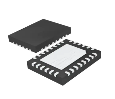
Specifications
Part Number Definition
ADG509A is a dual 4-channel differential CMOS analog multiplexer. K indicates standard industrial temperature grade. RZ stands for 16-lead narrow SOIC surface mount package. REEL7 refers to 7-inch tape-and-reel lead-free packaging designed for high-volume automated SMT assembly.
Core Electrical Performance Parameters
Fabricated with enhanced LC²MOS technology, this device incorporates two independent 4-channel single-pole four-throw switches for routing four differential analog signal pairs. Channel selection is realized via 2 address pins plus a global enable pin, with digital inputs fully compatible with TTL and 5V CMOS logic levels.
Flexible power supply options are available: single supply ranging from 10.8 V to 16.5 V, or dual bipolar supplies of ±10.8 V to ±16.5 V, with an absolute maximum voltage rating of 44 V. Analog input signals can swing rail-to-rail across the full supply range.
Maximum on-resistance is 450 Ω, with maximum on-resistance mismatch between channels limited to 22.5 Ω. Turn-on and turn-off switching times are both 300 ns, delivering fast channel transition speed. Off-state leakage current is typically 20 pA with a maximum value of 1 nA, which preserves measurement precision for low-level signals. Charge injection is only 4 pC, alongside low parasitic capacitance to minimize waveform distortion during signal switching.
Total maximum power dissipation is 28 mW for low quiescent power consumption. Internal frequency compensation ensures stable operation across all closed-loop configurations without external compensation components, suitable for low to medium frequency analog signal routing applications.
Packaging and Assembly Specifications
Housed in a compact 16-lead narrow SOIC plastic surface mount package with a body width of 3.9 mm, occupying minimal PCB layout area. Moisture Sensitivity Level is MSL1; no time limitation is imposed on reflow soldering after opening the vacuum sealed package. The 7-inch continuous tape-and-reel format seamlessly feeds automatic pick-and-place machinery for mass electronic manufacturing.
Environmental and Compliance Standards
Operating temperature range spans -40 °C to +85 °C, enabling continuous reliable operation inside industrial control cabinets, laboratory test instruments, outdoor monitoring terminals and other environments with wide temperature variation and electromagnetic interference. Manufactured using lead-free processes, the component complies with RoHS environmental directives. The fully integrated single-chip design eliminates numerous discrete peripheral components, simplifies the hardware design of differential analog acquisition frontends and accelerates product development cycles.
Typical Application Fields
Multi-channel differential sensor signal multiplexing circuits for industrial temperature and pressure process control
Front-end analog switching modules for high-precision DAQ data acquisition systems
Range selection circuitry for bench laboratory measuring instruments and digital multimeters
Multiplexed low-level signal sampling paths for portable inspection devices
Differential audio signal routing and analog conditioning circuits for compact medical diagnostic equipment


