





| Mfr Part | Datasheet | Series | Manufacturer | Package | Topology | Product Status | Mounting Type | Switching Frequency | Function | Input Voltage | Output Voltage | Number of Outputs | Operating Temperature | Output Type | Output Current |
|---|---|---|---|---|---|---|---|---|---|---|---|---|---|---|---|
| ADA4522-2ARZ-R7 |  |
ADA4522-2 | Analog Devices | 8-MSOP | Precision Op Amp | Active | Surface Mount | — | Low Noise Op Amp | ±4.5 V to ±18 V | Rail-to-Rail | 2 | −40°C to +125°C | Analog | — |
ADA4522-2ARZ-R7
Manufacturer: Analog Devices
Logic Cells: Dual zero-drift operational amplifier
Logic Slices: Ultra-low offset and drift architecture
Embedded RAM (eRAM): Internal precision bias and compensation circuitry
Package: SOIC-8
Operating Temperature: Industrial (-40 °C to +125 °C)
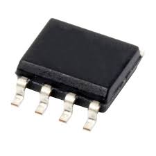
Specifications
Part Number Definition
ADA4522-2 is a dual-channel zero-drift, low-noise rail-to-rail input/output operational amplifier. ARZ stands for 8-lead narrow SOIC surface mount package. The suffix R7 refers to 7-inch lead-free tape-and-reel packaging intended for large-scale automated SMT assembly production.
Core Electrical Performance Parameters
This dual operational amplifier adopts auto-zero zero-drift architecture, delivering ultra-low DC offset and near-zero temperature drift, which perfectly fits precision DC signal amplification and low-frequency measurement scenarios. It supports both single supply and dual bipolar supply operation, with single supply ranging from 2.2 V to 5.5 V and dual supply spanning ±1.1 V to ±2.75 V.
The maximum input offset voltage is only 5 μV, and offset drift is less than 0.015 μV/°C across the entire temperature range. Input voltage noise reaches 8 nV/√Hz at 1 kHz, achieving an excellent balance between low noise and DC precision. The device features rail-to-rail input and output swing, making full use of the power supply voltage range and maximizing dynamic signal range under low-voltage working conditions.
Each channel consumes low quiescent current, which helps extend battery life for portable battery-powered devices. High common-mode rejection ratio and power supply rejection ratio effectively suppress power ripple and industrial common-mode interference. Internal integrated compensation circuitry ensures stable operation at unity gain without extra external compensation components. Channel crosstalk is extremely low to avoid mutual interference between two independent signal paths. The output stage can drive capacitive loads stably without oscillation.
Packaging and Assembly Specifications
Encapsulated in compact 8-pin narrow SOIC plastic surface mount package with small footprint, greatly saving PCB layout space for miniaturized analog front-end modules. Moisture Sensitivity Level is MSL3; all reflow soldering processes must be completed within 168 hours after the original vacuum packaging is opened. Continuous tape reel feeding mode is fully compatible with automatic pick-and-place equipment for mass electronic manufacturing lines.
Environmental and Compliance Standards
Industrial operating temperature range covers -40 °C to +125 °C, enabling long-term stable operation in industrial transmitters, portable precision measuring instruments, medical testing equipment and environmental monitoring sensors under severe temperature variation environments. Manufactured by lead-free processes, the component complies with global RoHS environmental directives. The dual-channel integrated design reduces the total number of components on PCB, simplifies multi-channel precision signal conditioning circuit layout and shortens hardware development cycles.
Typical Application Fields
Bridge sensor signal amplification for pressure, temperature and weighing measurement systems
Low-frequency tiny signal pre-amplification for portable data acquisition equipment
Precision voltage buffer and reference driving circuits for high-resolution ADC modules
Battery-powered handheld meters and field environmental monitoring instruments
Medical wearable device physiological signal conditioning and amplification circuits


