





| Mfr Part | Datasheet | Series | Manufacturer | Package | Topology | Product Status | Mounting Type | Switching Frequency | Function | Input Voltage | Output Voltage | Number of Outputs | Operating Temperature | Output Type | Output Current |
|---|---|---|---|---|---|---|---|---|---|---|---|---|---|---|---|
| AD9826KRSZRL |  |
AD9826 | Analog Devices | 28-SSOP | — | Active | Surface Mount | — | CCD Signal Processor | 3.0 V – 5.25 V | Analog | 1 | −40°C to +85°C | Analog | — |
AD9826KRSZRL
Manufacturer: Analog Devices
Logic Cells: Precision imaging signal conditioning IC
Logic Slices: 3-channel 16-bit ADC with CDS, gain and offset
Embedded RAM (eRAM): Internal analog processing blocks
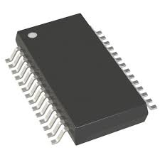
Package: SSOP-28
Operating Temperature: Industrial (-40 °C to +85 °C)
Specifications
Part Number Definition
AD9826 is a full integrated CCD signal analog front-end IC. K stands for industrial temperature grade specification. RSZ refers to 28-lead narrow SOIC surface mount package. RL means extended-length lead-free tape-and-reel packaging for uninterrupted high-volume automated SMT production.
Core Electrical Performance Parameters
This all-in-one analog frontend chip is exclusively designed for CCD image sensor signal acquisition and processing. It integrates correlated double sampling circuit, programmable gain amplifier, anti-aliasing low-pass filter and 16-bit ADC on a single die to complete the whole pixel signal conditioning and digitization workflow.
The built-in correlated double sampling circuit effectively suppresses CCD reset noise and dark noise, remarkably lifting overall image signal-to-noise ratio. The programmable gain amplifier supports continuous gain adjustment to adapt to varied illumination intensities and sensor output signal amplitudes. The on-chip low-pass filter cuts off out-of-band high frequency noise to avoid aliasing errors during analog-to-digital conversion.
The embedded 16-bit successive approximation ADC features excellent linearity and low differential non-linearity, delivering precise digital pixel output. The chip adopts dual power domain design: analog supply voltage ranges 2.7 V to 3.3 V, digital core and I/O supply supports 1.8 V ~ 3.3 V, compatible with mainstream FPGA and image processor power standards.
Internal serial interface is available for users to configure gain values, filter bandwidth, operating modes and power settings conveniently. Parallel digital bus outputs converted image data directly. Multiple power saving modes are provided; idle modules can be powered down to minimize quiescent power draw for battery-powered portable devices.
Packaging and Assembly Specifications
The component is housed in a 28-pin narrow SOIC plastic surface mount package with compact dimensions, taking up limited PCB space for compact scanner and vision hardware. Moisture Sensitivity Level is MSL3. All reflow soldering operations must be completed within 168 hours after the vacuum package is opened. Extended tape reel packaging enables continuous feeding for automatic placement equipment during mass production.
Environmental and Compliance Standards
Operating temperature range is -40 °C to +85 °C, enabling reliable long-term operation in document scanners, industrial machine vision equipment, optical measurement instruments and portable imaging devices under varying temperature and electromagnetic interference conditions. Produced with lead-free processes, the device complies with global RoHS environmental directives. High integration eliminates a large number of discrete peripheral analog components, greatly simplifying CCD camera circuit layout and shortening product development timeline.
Typical Application Fields
Flatbed scanners, film scanners and office document imaging equipment
Industrial CCD machine vision cameras for product surface inspection
Laboratory optical spectrum analysis and precision photometric measurement devices
Portable medical optical scanning diagnostic equipment
Low noise industrial surveillance camera analog signal processing frontends


