





| Mfr Part | Datasheet | Series | Manufacturer | Package | Topology | Product Status | Mounting Type | Switching Frequency | Function | Input Voltage | Output Voltage | Number of Outputs | Operating Temperature | Output Type | Output Current |
|---|---|---|---|---|---|---|---|---|---|---|---|---|---|---|---|
| AD8512ARZ |  |
— | Analog Devices | 8-SOIC | — | Active | Surface Mount | — | Precision Op Amp | 3 V – 36 V | Rail-to-Rail | 1 | −40°C to +125°C | Analog | — |
AD8512ARZ
Manufacturer: Analog Devices
Logic Cells: Precision operational amplifier
Logic Slices: Low offset voltage, low bias current design
Embedded RAM (eRAM): Internal precision analog circuitry
Package: SOIC-8
Operating Temperature: Industrial (-40 °C to +125 °C)
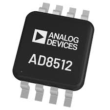
Specifications
Part Number Definition
AD8512 is a dual JFET input precision operational amplifier. ARZ stands for 8-lead narrow SOIC surface mount package, shipped in tube packaging for prototype testing and small batch production assembly.
Core Electrical Performance Parameters
This dual-channel monolithic operational amplifier combines ultra-low input bias current, high input impedance and superior DC precision, tailored for high impedance sensor signal conditioning and precision measurement circuits. It works with dual bipolar supplies ranging from ±5 V to ±18 V, and also supports single-supply operation.
The maximum input bias current is merely 25 pA at room temperature, which avoids loading effects on piezoelectric sensors, resistive bridge transducers and other high-impedance signal sources. Maximum input offset voltage is 0.25 mV, paired with low temperature drift to sustain stable DC accuracy across varying ambient temperatures.
Unity-gain bandwidth is 1 MHz, with fast settling time for step voltage signals. Low wideband noise and minimal harmonic distortion guarantee faithful amplification of faint analog waveforms without distortion. Internal integrated frequency compensation enables stable operation under all closed-loop gain configurations without external compensation components.
High common-mode rejection ratio and power supply rejection ratio effectively restrain power grid interference and common-mode noise in complex industrial electromagnetic environments. Excellent channel isolation suppresses crosstalk between the two independent amplifier channels. The output stage can steadily drive resistive loads while maintaining good linearity over the full output swing range. Total quiescent power consumption is kept low for continuous long-time running equipment.
Packaging and Assembly Specifications
Packaged in standard 8-pin narrow SOIC plastic surface mount housing with compact outline to conserve PCB layout space. Moisture Sensitivity Level is MSL3; all reflow soldering processes need to be completed within 168 hours after unsealing the original vacuum packaging. Tube delivery mode is adopted to facilitate manual breadboard debugging and small-volume instrument trial production.
Environmental and Compliance Standards
Operating temperature range extends from -40 °C to +85 °C, delivering reliable continuous performance inside industrial process instruments, desktop laboratory measuring devices and portable data acquisition terminals experiencing temperature fluctuations. Manufactured via lead-free production processes, the device complies with international RoHS environmental directives. The dual-amplifier single-chip design reduces the number of discrete components and simplifies dual-channel precision analog front-end circuit layout.
Typical Application Fields
High-impedance transducer dual-channel signal buffer and amplification circuits
Precision integrator, sample-and-hold analog modules for laboratory measurement equipment
Industrial strain gauge and pressure sensor signal conditioning units
Battery-powered portable multimeter and environmental monitoring instrument front ends
Audio preamplifier and low-frequency analog filtering circuits


