





| Mfr Part | Datasheet | Series | Manufacturer | Package | Topology | Product Status | Mounting Type | Switching Frequency | Function | Input Voltage | Output Voltage | Number of Outputs | Operating Temperature | Output Type | Output Current |
|---|---|---|---|---|---|---|---|---|---|---|---|---|---|---|---|
| AD8202YRZ |  |
AD8202 | Analog Devices | SOIC-8 | N/A | Active | Surface Mount | N/A | Current Sense Amplifier | 3 V – 5.5 V | N/A | 1 | −40°C to +125°C | Analog | N/A |
AD8202YRZ
Manufacturer: Analog Devices Inc.
Part: AD8202YRZ
Description: Single low-frequency differential amplifier / op-amp with broad utility in signal conditioning.
Key Specs: Single amplifier, differential inputs, general-purpose op-amp characteristics.
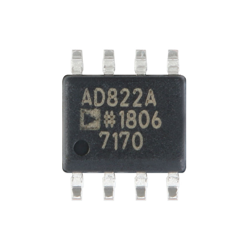
Specifications
Part Number Definition
AD8202 is a dual-channel low-cost rail-to-rail input and output CMOS operational amplifier. Y represents industrial temperature rating. RZ refers to 8-lead narrow SOIC surface mount package, shipped in tube packaging for prototype verification and small-batch production assembly.
Core Electrical Performance Parameters
This dual CMOS op amp is optimized for general-purpose low-voltage signal conditioning circuits. It supports single supply operation from 2.7 V to 5.5 V, and dual bipolar supplies ranging from ±1.35 V to ±2.75 V. Both input stage and output stage implement full rail-to-rail swing, maximizing available dynamic signal range under low supply voltage conditions.
Maximum input offset voltage is 1.5 mV, with gentle offset drift across changing temperatures. Unity-gain bandwidth reaches 3 MHz, accompanied by a slew rate of 1.3 V/μs, meeting the demands of low and medium frequency signal amplification. Input voltage noise is kept at a moderate level to balance power consumption and noise performance for common industrial measurement scenarios.
Each amplifier channel draws only 220 μA quiescent current, making the device ideal for battery-powered portable electronics to extend service time. On-chip internal frequency compensation guarantees unconditional stability at unity gain without external compensation components. High common-mode rejection ratio and power supply rejection ratio suppress power ripple and environmental electromagnetic interference effectively.
Crosstalk between the two independent amplifier channels is extremely low to avoid mutual signal interference. The output stage can drive small capacitive loads steadily without oscillation. No latch-up phenomenon occurs within the rated input voltage scope, ensuring reliable continuous operation.
Packaging and Assembly Specifications
Housed in a compact 8-pin narrow SOIC plastic surface mount package with small footprint, which saves PCB layout space for miniature sensor acquisition modules and portable circuit boards. Moisture Sensitivity Level is MSL3; all reflow soldering work must be finished within 168 hours once the vacuum sealed package is opened. Tube packaging facilitates manual breadboard debugging, parameter testing and small-volume trial production.
Environmental and Compliance Standards
Operating temperature range spans -40 °C to +125 °C, supporting long-term stable operation in industrial transmitters, handheld measuring meters, environmental monitoring sensors and consumer portable devices under fluctuating temperature conditions. Manufactured with lead-free processes, the component complies with global RoHS environmental directives. The dual-channel integrated layout reduces component count on printed circuit boards and simplifies multi-channel general analog front-end circuit design.
Typical Application Fields
Temperature, pressure and humidity sensor signal amplification circuits
Portable multimeters and field inspection instrument pre-amplifier modules
Active low-pass and high-pass filter circuits for low-frequency analog signals
Battery-powered IoT sensor node signal conditioning units
Consumer small household appliances control loop error amplifiers


