






| 모델 P/N | 시리즈 | 실험실/CLBS 수 | 속도 등급 | 논리 요소/셀 수 | 총 램 비트 | I/O 수 | 전압 - 공급 | 마운팅 유형 | 작동 온도 | 패키지 / 케이스 | 공급업체 디바이스 패키지 |
|---|---|---|---|---|---|---|---|---|---|---|---|
| XC7K480T-L2FFG1156E | 킨텍스-7 | 37.325,00 | -2,00 | 477,760 | 35205120 | 400 | 0.97 - 1.03V(통상 1.0V) | 표면 실장 | 0°C - 100°C | 1156-FCBGA | 1156-FCBGA(35×35mm) |
XC7K480T-L2FFG1156E
제조업체: 자일링스
로직 셀: 477,760
로직 슬라이스: 74,650
임베디드 RAM(eRAM): 33,840Kb(940 × 36Kb 블록 RAM)
최대 사용자 I/O: 500
패키지: FFG1156(플립칩 BGA)
속도 등급: -2L
작동 온도: 확장(0°C ~ +100°C)
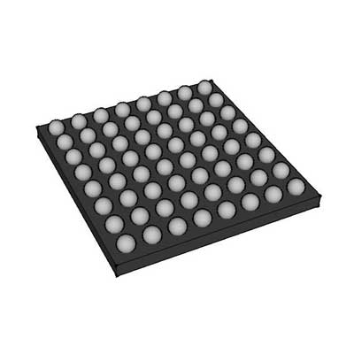
사양
Part Number Explanation
This is a low-power wide-temperature high-end large-scale FPGA belonging to Xilinx Kintex-7 product family, fabricated with mature 28nm semiconductor process. Equipped with ultra-rich logic, memory and DSP resources, it is optimized for low power consumption and wide temperature stability, widely deployed in airborne, vehicular, outdoor communication and precision portable test devices with strict power and thermal limitations.
- XC7K480T: High-end maximum-density model of Kintex-7 series; suffix T stands for low-power optimized silicon wafer version
- L2: Low-power optimized speed grade 2. The internal core voltage is properly reduced to lower static power and dynamic power consumption significantly. It maintains reliable timing performance across the full industrial temperature range while balancing operating frequency and power budget
- FFG1156: 1156-ball flip-chip FCBGA large package. Abundant pins provide enough expansion space for massive parallel I/O, multi-group high-speed transceivers and extended peripheral circuits
- E: 확장 산업용 온도 등급, 작동 접합 온도 범위: -40°C ~ +100°C
On-Chip Hardware Resource Parameters
1. General Programmable Logic Resources
- Total Logic Cells: 485,760
- Configurable Slices: 75,900
- Total Flip-Flops: 607,200
- Total LUTs: 303,600
2. Arithmetic and Embedded Memory Resources
- DSP48E1 arithmetic slices: 1,920 units, suitable for large-scale FFT operation, digital filtering, radar signal processing, multi-channel 4K video algorithm calculation and massive matrix computation tasks
- Total Block RAM capacity: 34,290 Kb, applied for large-capacity image frame buffering, deep FIFO data caching, waveform storage and algorithm parameter lookup tables
- Distributed RAM capacity: 8,440 Kb
3. Clock Management System
- 12 MMCM clock management tiles
- 12 PLL phase locked loops
It supports multi-clock domain generation, phase fine-tuning, clock delay compensation and high-frequency jitter suppression, meeting stringent synchronous timing requirements of ultra-large complex digital systems
4. 고속 직렬 트랜시버
- 20 GTX high-speed differential transceivers
Maximum transmission line rate up to 10.3125 Gbps, compatible with PCIe Gen2, 10 Gigabit Ethernet, CPRI, JESD204B, Aurora and other mainstream high-speed serial communication protocols
5. I/O Interfaces & On-Chip Monitoring Module
- Available user configurable I/O pins: 560
I/O bank voltage can be adjusted from 1.2V to 3.3V, fully compatible with LVCMOS, LVDS, HSTL, SSTL and all mainstream differential signal standards
A dual-channel 12-bit XADC analog monitor is integrated on chip, which monitors die junction temperature, all internal power supply voltages and external analog input signals in real time continuously
전원 공급 장치 사양
Low-power optimized core nominal voltage: 1.0V with power-saving tuning
Independent isolated power domains are configured for logic fabric, Block RAM, DSP array and high-speed transceivers respectively
Typical overall power consumption: 12W ~ 37W. Compact active cooling system can guarantee stable full-load operation under maximum temperature working conditions
포장 및 SMT 조립 요건
- Package form: 1156-pin flip-chip FCBGA ball grid array
- Moisture Sensitivity Level: MSL4; all reflow soldering processes must be finished within 72 hours after vacuum packaging is opened
- Lead-free structure, fully compliant with RoHS environmental directives
- Stored and shipped in anti-static trays to avoid electrostatic damage during automated PCB mass production
환경 적응성 및 신뢰성
The chip can operate stably for a long time under drastic temperature changes, mechanical vibration, impact and moderate electromagnetic interference harsh environments. It supports 256-bit AES bitstream encryption protection and SEU single-event upset detection and correction, with outstanding thermal robustness and anti-interference capability for long-term field deployment.
일반적인 애플리케이션 시나리오
- High-end portable spectrum analyzers, multi-channel high-speed oscilloscopes and signal acquisition recording equipment
- Software-defined radio baseband platforms, outdoor small cell wireless communication main control units
- Multi-channel industrial machine vision inspection systems, high-speed image real-time processing servers
- Vehicular multi-sensor fusion computing hosts, automotive intelligent edge computing terminals
- Light airborne radar signal preprocessing, flight data acquisition and forwarding modules
- Wide-temperature low-power high-performance industrial SOM core boards and ultra-complex embedded algorithm verification platforms


