






| MÃ SẢN PHẨM | BỘ PHIM | SỐ LƯỢNG PHÒNG THÍ NGHIỆM/CLBS | ĐỘ BỀN THEO TỐC ĐỘ | SỐ LƯỢNG PHẦN TỬ LỐI / TẾ BÀO | Tổng số bit RAM | SỐ LƯỢNG I/O | Điện áp – Nguồn cấp | Loại lắp đặt | NHIỆT ĐỘ HOẠT ĐỘNG | GÓI / HỘP | GÓI THIẾT BỊ CỦA NHÀ CUNG CẤP |
|---|---|---|---|---|---|---|---|---|---|---|---|
| XC7K480T-L2FFG1156E | Kintex-7 | 37.325,00 | -2,00 | 477,760 | 35205120 | 400 | 0,97 – 1,03 V (thông thường 1,0 V) | Lắp đặt bề mặt | 0 °C — 100 °C | 1156-FCBGA | 1156-FCBGA (35×35 mm) |
XC7K480T-L2FFG1156E
Nhà sản xuất: Xilinx
Tế bào logic: 477,760
Các lát cắt logic: 74,650
Bộ nhớ RAM tích hợp (eRAM): 33.840 Kb (940 × 36 Kb bộ nhớ RAM khối)
Dung lượng I/O tối đa của người dùng: 500
Gói: FFG1156 (BGA lật chip)
Đánh giá tốc độ: -2 lít
Nhiệt độ hoạt động: Mở rộng (0°C đến +100°C)
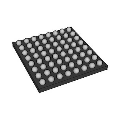
Thông số kỹ thuật
Giải thích về mã sản phẩm
Đây là một FPGA cao cấp, quy mô lớn, tiêu thụ điện năng thấp và hoạt động trong dải nhiệt độ rộng, thuộc dòng sản phẩm Xilinx Kintex-7, được sản xuất bằng quy trình bán dẫn 28nm đã được chứng minh. Được trang bị nguồn tài nguyên logic, bộ nhớ và DSP cực kỳ phong phú, sản phẩm này được tối ưu hóa để đạt mức tiêu thụ điện năng thấp và độ ổn định trong dải nhiệt độ rộng, được ứng dụng rộng rãi trong các thiết bị trên không, trên xe, hệ thống truyền thông ngoài trời và các thiết bị kiểm tra di động chính xác có các giới hạn nghiêm ngặt về điện năng và nhiệt độ.
- XC7K480T: Mẫu cao cấp có mật độ tích hợp tối đa thuộc dòng Kintex-7; hậu tố “T” biểu thị phiên bản tấm silicon được tối ưu hóa để tiết kiệm năng lượng
- L2: Cấp tốc độ 2 được tối ưu hóa cho mức tiêu thụ điện năng thấp. Điện áp lõi bên trong được giảm xuống mức phù hợp để giảm đáng kể mức tiêu thụ điện năng tĩnh và động. Cấp này duy trì hiệu suất đồng bộ hóa đáng tin cậy trong toàn bộ dải nhiệt độ công nghiệp, đồng thời cân bằng giữa tần số hoạt động và ngân sách điện năng.
- FFG1156: Gói FCBGA cỡ lớn 1156 chân sử dụng công nghệ flip-chip. Số lượng chân dồi dào cung cấp đủ không gian mở rộng cho các giao diện I/O song song quy mô lớn, các bộ thu phát tốc độ cao đa nhóm và các mạch ngoại vi mở rộng
- E: Loại chịu nhiệt độ công nghiệp mở rộng, dải nhiệt độ điểm nối hoạt động: -40°C ~ +100°C
Các tham số tài nguyên phần cứng trên chip
1. Các tài nguyên chung về logic lập trình được
- Tổng số ô logic: 485.760
- Số lát có thể cấu hình: 75.900
- Tổng số dép xỏ ngón: 607.200
- Tổng số LUT: 303.600
2. Các tài nguyên toán học và bộ nhớ nhúng
- Các khối tính toán của DSP48E1: 1.920 đơn vị, phù hợp cho các tác vụ FFT quy mô lớn, lọc tín hiệu số, xử lý tín hiệu radar, tính toán thuật toán video 4K đa kênh và các tác vụ tính toán ma trận quy mô lớn
- Tổng dung lượng RAM khối: 34.290 Kb, được sử dụng để đệm khung hình có dung lượng lớn, lưu trữ dữ liệu theo cơ chế FIFO sâu, lưu trữ dạng sóng và các bảng tra cứu tham số thuật toán
- Dung lượng RAM phân tán: 8.440 Kb
3. Hệ thống quản lý thời gian
- 12 khối quản lý đồng hồ MMCM
- 12 mạch khóa pha (PLL)
Nó hỗ trợ tạo nhiều miền đồng hồ, điều chỉnh pha chính xác, bù trễ đồng hồ và triệt tiêu dao động tần số cao, đáp ứng các yêu cầu nghiêm ngặt về đồng bộ thời gian của các hệ thống số phức tạp quy mô cực lớn
4. Bộ thu phát nối tiếp tốc độ cao
- 20 bộ thu phát vi sai tốc độ cao GTX
Tốc độ truyền dẫn tối đa lên đến 10,3125 Gbps, tương thích với PCIe Gen2, 10 Gigabit Ethernet, CPRI, JESD204B, Aurora và các giao thức truyền thông nối tiếp tốc độ cao phổ biến khác
5. Giao diện I/O và mô-đun giám sát trên chip
- Số chân I/O có thể cấu hình bởi người dùng: 560
Điện áp của khối I/O có thể điều chỉnh trong khoảng từ 1,2 V đến 3,3 V, hoàn toàn tương thích với các tiêu chuẩn LVCMOS, LVDS, HSTL, SSTL và tất cả các tiêu chuẩn tín hiệu vi sai phổ biến khác
Một bộ giám sát tương tự XADC 12-bit hai kênh được tích hợp trực tiếp trên chip, có chức năng giám sát liên tục và theo thời gian thực nhiệt độ điểm nối của chip, tất cả các điện áp nguồn bên trong và các tín hiệu đầu vào tương tự bên ngoài
Thông số kỹ thuật bộ nguồn
Điện áp danh định của lõi được tối ưu hóa cho chế độ tiêu thụ điện năng thấp: 1,0 V với cài đặt tiết kiệm năng lượng
Các vùng nguồn điện độc lập và cách ly được cấu hình lần lượt cho cấu trúc logic, Block RAM, mảng DSP và bộ thu phát tốc độ cao
Mức tiêu thụ điện năng tổng thể điển hình: 12W ~ 37W. Hệ thống làm mát chủ động nhỏ gọn có thể đảm bảo hoạt động ổn định ở tải đầy đủ trong điều kiện nhiệt độ làm việc tối đa
Yêu cầu về đóng gói và lắp ráp SMT
- Hình thức đóng gói: Mảng lưới bóng (FCBGA) loại flip-chip 1156 chân
- Mức độ nhạy cảm với độ ẩm: MSL4; tất cả các quy trình hàn nóng chảy phải được hoàn thành trong vòng 72 giờ sau khi mở bao bì chân không
- Cấu trúc không chứa chì, tuân thủ hoàn toàn các chỉ thị môi trường RoHS
- Được bảo quản và vận chuyển trong các khay chống tĩnh điện để tránh hư hỏng do tĩnh điện trong quá trình sản xuất hàng loạt PCB tự động
Khả năng thích ứng với môi trường và độ tin cậy
Con chip này có thể hoạt động ổn định trong thời gian dài trong các môi trường khắc nghiệt với sự thay đổi nhiệt độ đột ngột, rung động cơ học, va đập và nhiễu điện từ ở mức vừa phải. Nó hỗ trợ bảo vệ mã hóa luồng bit AES 256-bit và tính năng phát hiện và sửa lỗi SEU (Single-Event Upset), đồng thời sở hữu độ bền nhiệt và khả năng chống nhiễu vượt trội, phù hợp cho việc triển khai lâu dài tại hiện trường.
Các tình huống ứng dụng điển hình
- Máy phân tích phổ cầm tay cao cấp, máy hiện sóng đa kênh tốc độ cao và thiết bị thu thập và ghi lại tín hiệu
- Nền tảng băng tần cơ sở của hệ thống vô tuyến định nghĩa bằng phần mềm, các đơn vị điều khiển chính cho hệ thống truyền thông không dây tế bào nhỏ ngoài trời
- Hệ thống kiểm tra bằng thị giác máy công nghiệp đa kênh, máy chủ xử lý hình ảnh thời gian thực tốc độ cao
- Các thiết bị chủ xử lý tích hợp đa cảm biến trên phương tiện giao thông, các thiết bị đầu cuối tính toán biên thông minh trong ngành ô tô
- Các mô-đun tiền xử lý tín hiệu radar trên không nhẹ, thu thập dữ liệu bay và chuyển tiếp dữ liệu
- Các bo mạch lõi SOM công nghiệp hiệu suất cao, tiêu thụ điện năng thấp, hoạt động trong dải nhiệt độ rộng và các nền tảng xác minh thuật toán nhúng cực kỳ phức tạp


