






| MODEL P / N | SERI | JUMLAH LABORATORIUM/CLBS | TINGKAT KECEPATAN | JUMLAH ELEMEN / SEL LOGIKA | TOTAL BIT RAM | JUMLAH I / O | TEGANGAN - PASOKAN | JENIS PEMASANGAN | SUHU PENGOPERASIAN | PAKET / KASUS | PAKET PERANGKAT PEMASOK |
|---|---|---|---|---|---|---|---|---|---|---|---|
| XC7K480T-L2FFG1156E | Kintex-7 | 37.325,00 | -2,00 | 477,760 | 35205120 | 400 | 0,97 - 1,03 V (ketik 1,0 V) | Pemasangan di permukaan | 0 ° C - 100 ° C | 1156-FCBGA | 1156-FCBGA (35×35 mm) |
XC7K480T-L2FFG1156E
Produsen: Xilinx
Sel Logika: 477,760
Irisan Logika: 74,650
RAM tertanam (eRAM): 33.840 Kb (940 × 36Kb Blok RAM)
I/O Pengguna Maksimum: 500
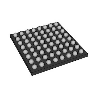
Paket: FFG1156 (Flip-Chip BGA)
Tingkat Kecepatan: -2L
Suhu Pengoperasian: Diperpanjang (0°C hingga +100°C)
Spesifikasi
Penjelasan Nomor Bagian
Ini adalah FPGA berskala besar kelas atas dengan konsumsi daya rendah dan rentang suhu luas yang termasuk dalam keluarga produk Xilinx Kintex-7, yang diproduksi menggunakan proses semikonduktor 28 nm yang telah teruji. Dilengkapi dengan sumber daya logika, memori, dan DSP yang sangat melimpah, perangkat ini dioptimalkan untuk konsumsi daya rendah dan stabilitas suhu yang luas, serta banyak digunakan dalam aplikasi penerbangan, kendaraan, komunikasi luar ruangan, dan perangkat pengujian portabel presisi yang memiliki batasan daya dan termal yang ketat.
- XC7K480T: Model kelas atas dengan kepadatan maksimum dari seri Kintex-7; sufiks T menunjukkan versi wafer silikon yang dioptimalkan untuk konsumsi daya rendah
- L2: Tingkat kecepatan 2 yang dioptimalkan untuk konsumsi daya rendah. Tegangan inti internal diturunkan secara tepat untuk mengurangi konsumsi daya statis dan dinamis secara signifikan. Hal ini memastikan kinerja timing yang andal di seluruh rentang suhu industri, sekaligus menjaga keseimbangan antara frekuensi operasi dan anggaran daya
- FFG1156: Kemasan besar FCBGA flip-chip dengan 1156 bola. Jumlah pin yang melimpah menyediakan ruang ekspansi yang cukup untuk I/O paralel berskala besar, transceiver berkecepatan tinggi multi-kelompok, dan sirkuit periferal yang diperluas
- E: Kelas suhu industri yang diperluas, rentang suhu sambungan operasional: -40°C ~ +100°C
Parameter Sumber Daya Perangkat Keras pada Chip
1. Sumber Daya Umum tentang Logika yang Dapat Diprogram
- Jumlah Sel Logika: 485.760
- Potongan yang Dapat Dikonfigurasi: 75.900
- Jumlah Sandal Jepit: 607.200
- Jumlah LUT: 303.600
2. Sumber Daya Aritmatika dan Memori Tertanam
- Slice aritmatika DSP48E1: 1.920 unit, cocok untuk operasi FFT berskala besar, penyaringan digital, pemrosesan sinyal radar, perhitungan algoritma video 4K multi-saluran, dan tugas-tugas komputasi matriks berskala besar
- Total kapasitas RAM Blok: 34.290 Kb, digunakan untuk penyimpanan sementara bingkai gambar berkapasitas besar, penyimpanan data FIFO mendalam, penyimpanan bentuk gelombang, dan tabel pencarian parameter algoritma
- Kapasitas RAM terdistribusi: 8.440 Kb
3. Sistem Manajemen Waktu
- 12 modul pengelolaan jam MMCM
- 12 sirkuit pengunci fase (PLL)
Fitur ini mendukung pembangkitan domain clock ganda, penyetelan fase yang presisi, kompensasi penundaan clock, dan penekanan jitter frekuensi tinggi, sehingga memenuhi persyaratan waktu sinkron yang ketat pada sistem digital kompleks berskala sangat besar
4. Transceiver Serial Berkecepatan Tinggi
- 20 transceiver diferensial berkecepatan tinggi tipe GTX
Kecepatan maksimum jalur transmisi hingga 10,3125 Gbps, kompatibel dengan PCIe Gen2, 10 Gigabit Ethernet, CPRI, JESD204B, Aurora, dan protokol komunikasi serial berkecepatan tinggi populer lainnya
5. Antarmuka I/O & Modul Pemantauan Terintegrasi
- Jumlah pin I/O yang dapat dikonfigurasi oleh pengguna: 560
Tegangan bank I/O dapat disesuaikan dari 1,2 V hingga 3,3 V, dan sepenuhnya kompatibel dengan LVCMOS, LVDS, HSTL, SSTL, serta semua standar sinyal diferensial yang umum digunakan
Sebuah monitor analog XADC 12-bit saluran ganda terintegrasi dalam chip, yang secara terus-menerus memantau suhu sambungan chip, semua tegangan catu daya internal, dan sinyal masukan analog eksternal secara real-time
Spesifikasi Catu Daya
Tegangan nominal inti yang dioptimalkan untuk konsumsi daya rendah: 1,0 V dengan pengaturan hemat daya
Domain daya terisolasi yang independen dikonfigurasi masing-masing untuk struktur logika, Block RAM, susunan DSP, dan transceiver berkecepatan tinggi
Konsumsi daya keseluruhan yang umum: 12W ~ 37W. Sistem pendingin aktif yang ringkas dapat menjamin pengoperasian beban penuh yang stabil dalam kondisi suhu kerja maksimum
Persyaratan Pengemasan & Perakitan SMT
- Bentuk kemasan: FCBGA (ball grid array) flip-chip 1156-pin
- Tingkat Sensitivitas Kelembapan: MSL4; semua proses penyolderan reflow harus diselesaikan dalam waktu 72 jam setelah kemasan vakum dibuka
- Struktur bebas timbal, sepenuhnya sesuai dengan arahan lingkungan RoHS
- Disimpan dan dikirim dalam baki antistatis untuk mencegah kerusakan akibat muatan listrik statis selama proses produksi massal PCB secara otomatis
Kemampuan Beradaptasi terhadap Lingkungan & Keandalan
Chip ini dapat beroperasi secara stabil dalam jangka waktu lama di lingkungan yang ekstrem, seperti perubahan suhu yang drastis, getaran mekanis, benturan, serta gangguan elektromagnetik sedang. Chip ini mendukung perlindungan enkripsi bitstream AES 256-bit serta deteksi dan koreksi SEU (Single-Event Upset), dengan ketahanan termal dan kemampuan anti-gangguan yang luar biasa untuk penerapan jangka panjang di lapangan.
Skenario Aplikasi Umum
- Analisis spektrum portabel kelas atas, osiloskop multikanal berkecepatan tinggi, dan peralatan perekaman serta akuisisi sinyal
- Platform pita dasar radio yang ditentukan oleh perangkat lunak, unit pengendali utama komunikasi nirkabel sel kecil luar ruangan
- Sistem inspeksi visi mesin industri multi-saluran, server pemrosesan gambar berkecepatan tinggi secara real-time
- Host komputasi fusi multisensor kendaraan, terminal komputasi tepi cerdas otomotif
- Modul prapemrosesan sinyal radar udara ringan, pengumpulan data penerbangan, dan penerusan data
- Papan inti SOM industri berkinerja tinggi, berdaya rendah, dan tahan rentang suhu luas, serta platform verifikasi algoritma tertanam yang sangat kompleks


