






| MODEL P / N | SERI | JUMLAH LABORATORIUM/CLBS | TINGKAT KECEPATAN | JUMLAH ELEMEN / SEL LOGIKA | TOTAL BIT RAM | JUMLAH I / O | TEGANGAN - PASOKAN | JENIS PEMASANGAN | SUHU PENGOPERASIAN | PAKET / KASUS | PAKET PERANGKAT PEMASOK |
|---|---|---|---|---|---|---|---|---|---|---|---|
| XCVU13P-1FHGC2104I | XCVU13P (Virtex US+) | 216,00 | -1,00 | 3.780.000 LE | 514.867.200 bit | 416 | ~0.698-0.876 V | Pemasangan di Permukaan (BGA) | Industri (-40°C hingga +100°C) | 2104 FCBGA | 2104-FCBGA (FBGA-2104). . |
XCVU13P-1FHGC2104I
Produsen: Xilinx
Sel Logika: 13,140,000
Irisan Logika: 2,050,000
RAM tertanam (eRAM): 94,320 Kb (2,620 × 36Kb Block RAM)
I/O Pengguna Maksimum: 800
Paket: FHGC2104 (Flip-Chip BGA)
Tingkat Kecepatan: -1
Suhu Pengoperasian: Industri (-40°C hingga +100°C)
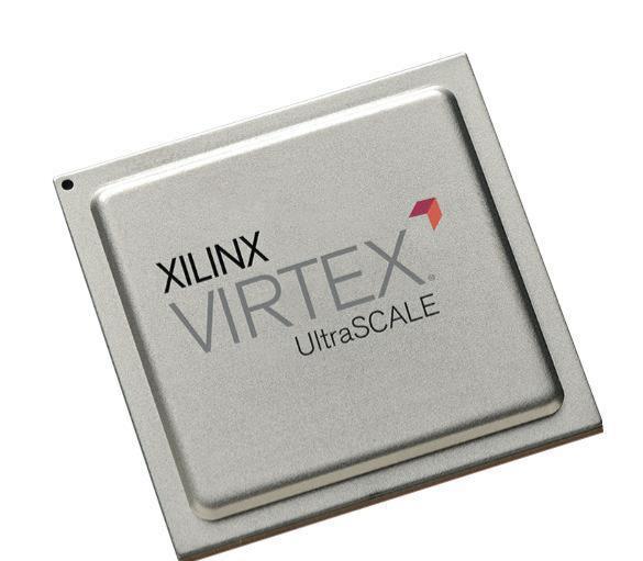
Spesifikasi
Definisi Nomor Bagian
This industrial temperature low-power FPGA belongs to Xilinx Virtex UltraScale+ family, fabricated on 16nm FinFET process. It adopts upgraded UltraScale+ architecture with optimized power efficiency, equipped with balanced logic, arithmetic, storage and high-speed serial resources. It is designed for battery-powered portable field devices, miniature airborne payload systems, vehicular embedded computing units and outdoor industrial signal processing equipment that need reliable operation across the complete industrial temperature range.
- XCVU13P: Mid-range capacity device of Virtex UltraScale+ series, the P suffix stands for power-optimized variant with enhanced low-power performance and refined on-chip interconnection structure
- -1: Speed Grade 1, low-power oriented timing grade. Thermal stability and power consumption control take precedence over maximum clock frequency, perfectly fit long-term continuous running hardware with limited heat dissipation space
- FHGC2104: 2104-ball flip-chip FCBGA package. Abundant pins support full layout of all integrated transceivers, large-scale general I/O arrangement and multi-channel high-speed memory interface connection while keeping the overall device compact
- I: Industrial temperature specification, continuous junction temperature working range: -40°C ~ +100°C
Rincian Sumber Daya Perangkat Keras pada Chip
1. Sumber Daya Logika yang Dapat Diprogram
- Total System Logic Cells: 1488000
- Configurable CLB Slices: 84960
- Total Flip-Flops: 1699200
- Total LUT Lookup Tables: 84960
- Distributed RAM Capacity: 12.4 Mb
2. Sumber Daya Aritmatika dan Memori Tertanam
- DSP48E3 arithmetic computing blocks: 1128 units, optimized for floating-point and fixed-point operations, large-scale FFT calculation, communication baseband processing, radar signal modulation and cryptographic algorithm acceleration, suitable for medium-sized matrix computing tasks
- Total Block RAM Capacity: 41.8 Mb, used for image frame buffering, deep FIFO data caching, waveform data storage and algorithm parameter lookup tables
No embedded UltraRAM inside this chip
3. Clock Management Subsystem
- 14 MMCM clock management tiles
- 14 PLL phase-locked loops
Multiple mutually independent clock domains can be configured flexibly. The module supports accurate clock phase adjustment, signal transmission delay compensation and ultra-low jitter suppression, meeting strict synchronous timing requirements of complex large-scale digital systems
4. Transceiver Serial Berkecepatan Tinggi
- 28 GTH differential high-speed transceivers
Each lane maximum transmission rate reaches 32.75 Gbps, compatible with PCIe Gen4, 100G Ethernet, Aurora, JESD204B and other mainstream high-speed serial communication protocols. Built-in hard MAC controllers simplify high-bandwidth network interface development work
5. I/O Interfaces and System Monitoring Module
- Configurable user I/O pins: 912
Multiple I/O bank voltage domains cover 1.2V to 3.3V, fully compatible with LVCMOS, LVDS, HSTL, SSTL and all conventional single-ended and differential signal standards
The built-in system monitoring module collects chip junction temperature, internal power supply voltages and external analog input signals in real time continuously
Power Supply Characteristics
Speed Grade 1 features optimized low-power core voltage ranging from 0.82V to 0.88V. Programmable logic area, block RAM, DSP arrays and serial transceivers adopt independent power domains, supporting partial module power gating to flexibly reduce overall power consumption
Typical total power consumption ranges from 13W to 44W. For stable full-load continuous operation under the upper industrial temperature limit, forced air cooling configuration is required
Packaging and SMT Assembly Specifications
- Package form: 2104-pin FCBGA flip-chip ball grid array
- Moisture Sensitivity Level: MSL4. All reflow soldering procedures must be completed within 72 hours after vacuum packaging is opened
- Lead-free packaging design, fully compliant with RoHS environmental standards
- Devices are stored and transported in anti-static trays to prevent electrostatic damage during mass PCB assembly production
Environmental Adaptability and Operational Reliability
The chip can run stably for a long time under severe temperature fluctuation, mechanical shock, vibration and strong electromagnetic interference environments. It supports AES bitstream encryption, dynamic partial reconfiguration, SEU single-event upset detection and correction, with upgraded radiation resistance, applicable to aerospace miniature payload equipment, military portable measuring terminals and outdoor industrial field deployment scenarios
Skenario Aplikasi Umum
- Lightweight unmanned aerial vehicle payload computing boards and miniature airborne signal preprocessing modules
- Compact military rugged VPX embedded auxiliary control mainboards
- Portable field spectrum analyzers and outdoor arbitrary waveform signal generators
- Outdoor industrial multi-channel sensor data acquisition and real-time signal processing systems
- Medium-scale chip prototype verification platforms with strict power and space constraints
- Vehicular intelligent perception data fusion units and wide-temperature industrial edge gateways


