






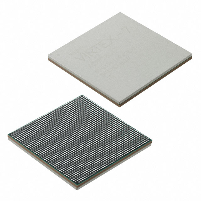
XC7VX690T-2FFG1927I
Fabricante: AMD (Xilinx)
Células lógicas: 693,120
Rebanadas lógicas: 108,300
RAM integrada (eRAM): 52,920 Kb (2,940 × 18Kb Block RAM)
Paquete: FFG1927 (Flip-Chip BGA)
Temperatura de funcionamiento: Industrial (-40°C a +100°C)
Especificaciones
Part Number Detailed Definition
This is AMD Xilinx Virtex-7 series high-capacity signal processing FPGA, built on 28nm HKMG process, tailored for large-scale real-time signal processing, high-speed data interconnection and high-precision measurement equipment.
- XC7VX690T: Virtex-7 VX series flagship large-capacity chip optimized for digital signal processing
- -2: Speed Grade 2, high-performance timing grade with ample timing margin for complex high-speed logic design
- FFG1927: 1927-ball FCBGA flip-chip ball grid array package
- I: Industrial temperature grade, junction temperature operating range: -40°C ~ +100°C
Core On-Chip Hardware Resources
Logic & DSP Arithmetic Resources
- Total Logic Cells: 693,120
- Configurable Logic Slices: 108,300
- DSP48E1 dedicated arithmetic slices: 3,600 units, extensively used for FFT, digital filtering, matrix computation, radar echo processing and multiply-accumulate intensive algorithms
Recursos de memoria integrada
- Total Block RAM capacity: 52.92 Mbit, composed of independent dual-port RAM blocks for large-capacity data buffering, FIFO and algorithm intermediate storage
- LUT-based distributed RAM for low-latency small temporary data cache
Módulos de gestión de reloj
14 sets of CMT clock management tiles are integrated. Each tile contains one MMCM + one PLL module, supporting clock frequency multiplication/division, arbitrary phase adjustment and jitter attenuation to satisfy the clock demands of multi-clock ultra-high-speed digital systems.
Transceptores seriales de alta velocidad y E/S general
- 80-channel GTX high-speed differential transceivers, maximum single-lane transmission rate up to 12.5 Gbps
Compatible protocols: PCIe Gen2, 10G Ethernet, Serial RapidIO, Aurora, high-speed inter-board data transmission
- Total available user general I/O pins: 840
- Supports LVCMOS, LVDS, differential signaling and all mainstream industrial electrical level standards
System Monitoring Module
Built-in XADC analog monitor, which can collect chip internal junction temperature, multi-group core power supply voltage and external analog input signals in real time.
Especificaciones de la fuente de alimentación
- Core digital nominal voltage: 1.0 V
- Each I/O bank supports configurable voltage: 1.2V / 1.5V / 1.8V / 2.5V / 3.3V
- Typical full-load overall power consumption: 65W ~ 110W, requires forced air cooling or liquid cooling heat dissipation scheme
Requisitos de empaque y ensamblaje SMT
- Package form: 1927-pin flip-chip FCBGA surface mount package
- Moisture Sensitivity Level: MSL3; all reflow soldering processes must be finished within 168 hours once vacuum packaging is opened
- Empaque totalmente libre de plomo, que cumple con las directivas ambientales globales de la RoHS
- Standard shipping: anti-static tray packaging for automated industrial PCB mass production
Environmental & Reliability Characteristics
Stable continuous operation under severe temperature variation and strong electromagnetic interference environments.
Supports 256-bit AES bitstream encryption for design IP protection, SEU radiation error correction and partial dynamic reconfiguration functions, suitable for long-term uninterrupted operation of military, aerospace and industrial high-end equipment.
Campos de aplicación típicos
- Phased array radar, electronic warfare large-scale real-time signal processing platforms
- Communication base station massive MIMO baseband processing and high-speed data forwarding equipment
- High-end oscilloscopes, spectrum analyzers and ultra-high-speed transient signal recording instruments
- Aerospace remote sensing massive data real-time processing, onboard embedded computing systems
- High-speed data acquisition cards, large-scale parallel DSP acceleration arrays
- High-performance computing acceleration boards, custom high-bandwidth data gateway devices


