






| MODELO P/N | SERIE | NÚMERO DE LABORATORIOS/CLBS | GRADO DE VELOCIDAD | NÚMERO DE ELEMENTOS LÓGICOS / CELDAS | TOTAL BITS RAM | NÚMERO DE E/S | TENSIÓN - ALIMENTACIÓN | TIPO DE MONTAJE | TEMPERATURA DE FUNCIONAMIENTO | PAQUETE / ESTUCHE | PAQUETE DEL DISPOSITIVO DEL PROVEEDOR |
|---|---|---|---|---|---|---|---|---|---|---|---|
| XC7K480T-2FFG1156E | Kintex-7 | 37.325,00 | -2,00 | 477,760 | 35205120 | 400 | 0,97 – 1,03 V (típico: 1,0 V) | Montaje en superficie | 0 °C — 100 °C | 1156-FCBGA | 1156-FCBGA (35 × 35 mm) |
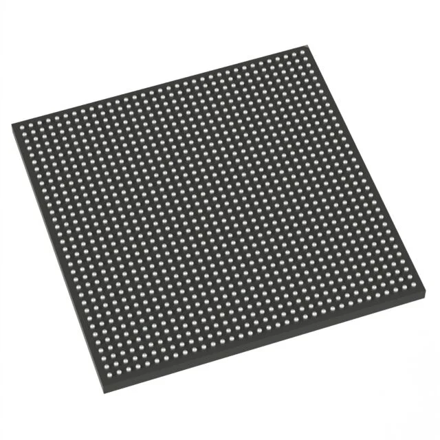
XC7K480T-2FFG1156E
Fabricante: Xilinx
Células lógicas: 477,760
Rebanadas lógicas: 74,650
RAM integrada (eRAM): 33 840 Kb (940 × 36 Kb de RAM en bloques)
E/S máxima por usuario: 500
Paquete: FFG1156 (BGA con chip invertido)
Grado de velocidad: -2
Temperatura de funcionamiento: Ampliado (0 °C a +100 °C)
Especificaciones
Definición del número de pieza
Este FPGA de alta densidad y rango de temperatura industrial ampliado pertenece a la familia Kintex-7 de Xilinx, fabricado con un proceso semiconductor maduro de 28 nm. Ofrece abundantes recursos lógicos, de procesamiento de señal digital (DSP) y de almacenamiento, junto con numerosas interfaces seriales de alta velocidad, diseñadas para el procesamiento complejo de señales, la adquisición de datos multicanal a alta velocidad, la visión industrial y los equipos de comunicación resistentes que requieren un funcionamiento estable en un amplio rango de temperaturas industriales.
- XC7K480T: Modelo de alta capacidad de gama alta de la serie Kintex-7; el sufijo T se refiere a una variante de silicio optimizada para bajo consumo
- -2: Grado de velocidad 2, grado de sincronización equilibrado estándar. Reserva un margen de sincronización suficiente para el diseño de lógica digital a gran escala y de alta frecuencia, equilibrando la frecuencia máxima de operación, la estabilidad del cierre de sincronización y el consumo de energía total
- FFG1156: Paquete grande FCBGA de 1156 bolas con tecnología flip-chip. Su gran número de pines permite una amplia expansión periférica, acceso paralelo a señales multicanal y el aprovechamiento total de los transceptores integrados.
- E: Especificación de temperatura industrial ampliada, rango de temperatura de unión en funcionamiento: -40 °C a +100 °C
Detalles de los recursos de hardware integrados en el chip
1. Recursos generales sobre lógica programable
- Total de celdas lógicas: 485 760
- Segmentos configurables: 75 900
- Total de flip-flops: 607 200
- Total de LUT: 303 600
2. Recursos aritméticos y de memoria integrada
- Módulos aritméticos del DSP48E1: 1920 unidades, ideales para cálculos de FFT a gran escala, filtrado digital, demodulación de señales de radar, aceleración de algoritmos de video multicanal de alta definición y operaciones con matrices grandes
- Capacidad total de la memoria RAM en bloque: 34 290 Kb, utilizada para el almacenamiento en caché de fotogramas de imagen, el almacenamiento en búfer de datos FIFO profundo, el almacenamiento de formas de onda y las tablas de consulta de parámetros de algoritmos
- Capacidad de RAM distribuida: 8440 Kb
3. Subsistema de gestión del reloj
- 12 bloques de gestión de reloj MMCM
- 12 circuitos de bucle de fase (PLL)
Admite la generación de múltiples dominios de reloj, el ajuste de fase, la compensación de retrasos de reloj y la supresión de fluctuaciones de alta frecuencia, lo que cumple con los estrictos requisitos de sincronización temporal de los sistemas embebidos complejos y de gran tamaño.
4. Transceptores seriales de alta velocidad
- 20 transceptores diferenciales de alta velocidad GTX
Velocidad máxima de línea de hasta 10,3125 Gbps, compatible con los protocolos de comunicación en serie más comunes: PCIe Gen2, 10 Gigabit Ethernet, CPRI, JESD204B y Aurora
5. Interfaces de E/S y módulo de monitoreo integrado en el chip
- Pines de E/S configurables para el usuario: 560
Voltaje del banco de E/S ajustable de 1,2 V a 3,3 V, totalmente compatible con LVCMOS, LVDS, HSTL, SSTL y todos los estándares de señal diferencial más comunes
Monitor analógico XADC integrado de doble canal y 12 bits para realizar un monitoreo continuo en tiempo real de la temperatura de unión del chip, los voltajes de la fuente de alimentación interna y las señales de entrada analógicas externas
Especificaciones de la fuente de alimentación
Tensión nominal de funcionamiento del núcleo: 1,0 V
La estructura lógica, la memoria RAM en bloque, la matriz DSP y los transceptores seriales adoptan dominios de alimentación independientes y aislados por separado
Consumo energético total típico: 13 W ~ 38 W; se requiere un sistema de enfriamiento activo por aire forzado para un funcionamiento continuo y estable a plena carga en condiciones de temperatura límite elevadas
Requisitos de empaque y ensamblaje SMT
- Tipo de paquete: FCBGA (matriz de bolas) de 1156 pines con tecnología flip-chip
- Nivel de sensibilidad a la humedad: MSL4; todos los procesos de soldadura por reflujo deben completarse en un plazo de 72 horas después de abrir el empaque al vacío
- Fabricación sin plomo, que cumple plenamente con las directivas ambientales de la RoHS
- Se entregan y almacenan en bandejas antiestáticas para evitar daños electrostáticos durante la producción automatizada en masa de placas de circuito impreso
Adaptabilidad ambiental y confiabilidad
El chip mantiene un funcionamiento estable a largo plazo en entornos industriales exigentes, sujetos a amplias fluctuaciones de temperatura, vibraciones mecánicas, golpes e interferencias electromagnéticas moderadas. Es compatible con el cifrado de flujo de bits AES de 256 bits y con la detección y corrección de errores de evento único (SEU), y cuenta con una excelente resistencia térmica y un alto rendimiento antiinterferencias para dispositivos resistentes de uso en el campo.
Escenarios típicos de aplicación
- Analizadores de espectro portátiles de alta gama, osciloscopios multicanal de alta velocidad e instrumentos de registro de señales transitorias
- Plataformas de procesamiento de banda base de radio definida por software; equipo de control principal para comunicaciones inalámbricas de células pequeñas en exteriores
- Sistemas industriales de inspección por visión artificial multicanal; unidades de procesamiento de imágenes en tiempo real a alta velocidad
- Puerta de enlace industrial de alto rendimiento, equipo de integración de buses de campo multiprotocolo
- Módulos ligeros de preprocesamiento de señales de radar aerotransportado; hosts de cómputo para la fusión multisensor montados en vehículos
- Placas base SOM industriales de alto rendimiento para rangos de temperatura ampliados y plataformas de verificación de prototipos de algoritmos integrados ultracomplejos


