






| МОДЕЛЬ П/Н | СЕРИИ | КОЛИЧЕСТВО ЛАБОРАТОРИЙ/КЛБ | УРОВЕНЬ СКОРОСТИ | КОЛИЧЕСТВО ЛОГИЧЕСКИХ ЭЛЕМЕНТОВ / ЯЧЕЕК | ВСЕГО БИТОВ ОЗУ | КОЛИЧЕСТВО ВХОДОВ/ВЫХОДОВ | НАПРЯЖЕНИЕ - ПИТАНИЕ | ТИП КРЕПЛЕНИЯ | РАБОЧАЯ ТЕМПЕРАТУРА | УПАКОВКА / КЕЙС | УПАКОВКА УСТРОЙСТВА ПОСТАВЩИКА |
|---|---|---|---|---|---|---|---|---|---|---|---|
| XCKU095-1FFVC1517I | Kintex® UltraScale | 67,20 | -1,00 | 1,176,000 LE | 60518400 | 520 | 0,922 V ~ 0,979 V | Монтаж на поверхность | -40 °C ~ +100 °C (I класс) | 1517-FCBGA | 1517-FCBGA |
XCKU095-1FFVC1517I
Производитель: Xilinx
Логические ячейки: 1,143,360
Логические срезы: 178,650
Встроенная оперативная память (eRAM): 48 960 Кб (1 360 × 36 Кб блочной оперативной памяти)
Максимальный пользовательский ввод/вывод: 520
Упаковка: FFVC1517 (Flip-Chip BGA)
Класс скорости: -1
Рабочая температура: Промышленные (от -40°C до +100°C)
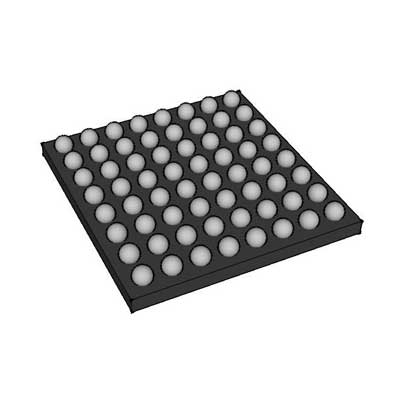
Технические характеристики
Определение номера детали
This industrial temperature low-power FPGA belongs to AMD Xilinx Kintex UltraScale series, manufactured on mature 20nm FinFET process technology. It adopts balanced-performance UltraScale architecture, focusing on the combination of computing capacity, high-speed serial bandwidth and power efficiency. It is widely applied in outdoor industrial signal processing, wireless communication baseband modules, vehicle-mounted embedded computing equipment, portable field test instruments and miniature ruggedized airborne devices requiring reliable continuous operation across full industrial temperature range.
- XCKU095: Mid-high capacity mainstream device of Kintex UltraScale lineup. Kintex series is positioned between Artix and Virtex, striking a perfect balance between performance, power consumption and cost for industrial and communication scenarios
- -1: Speed Grade 1, the slowest low-power timing grade of this series. Power consumption reduction and thermal stability are prioritized over maximum operating frequency, suitable for long-term continuous running hardware with limited heat dissipation space
- FFVC1517: 1517-ball compact flip-chip FCBGA package, physical size 40mm × 40mm. The compact outline facilitates equipment miniaturization, while sufficient pins support complete layout of all integrated GTH transceivers, general-purpose I/O circuits and multi-channel DDR4 memory interfaces
- I: Industrial temperature grade, continuous junction temperature operating range: -40°C ~ +100°C
Параметры аппаратных ресурсов на кристалле
1. Ресурсы по программируемой логике
- Total System Logic Cells: 1176000
- Configurable CLB Slices: 67200
- Total Flip-Flops: 1075200
- Total LUT Lookup Tables: 537600
- Distributed RAM Capacity: 8.4 Mb
2. Арифметические ресурсы и ресурсы встроенной памяти
- DSP48E2 arithmetic blocks: 768 units, dedicated to fixed-point/floating-point calculation, large-scale FFT spectrum analysis, wireless baseband signal processing, radar echo decoding and cryptographic algorithm acceleration tasks
- Total Block RAM Capacity: 59.1 Mb, used for image frame buffering, deep FIFO data caching, waveform raw data storage and algorithm parameter lookup tables
No UltraRAM memory is embedded inside this chip
3. Подсистема управления часами
- 14 MMCM clock management tiles
- 14 PLL phase-locked loops
Multiple mutually independent clock domains can be freely configured. The subsystem supports precise clock phase shifting, signal transmission delay compensation and high-frequency jitter suppression, meeting strict synchronous timing requirements of medium-to-large communication and digital signal processing systems
4. Высокоскоростные последовательные приемопередатчики
- 32 GTH differential high-speed transceivers
Each lane supports maximum transmission rate of 16.3 Gbps, compatible with PCIe Gen3, 100G Ethernet, Aurora, JESD204B and mainstream industrial serial communication protocols. Built-in hard protocol controllers greatly shorten the development cycle of high-speed data transmission interfaces
5. I/O Interfaces and System Monitoring Module
- Configurable user I/O pins: 520
Multiple I/O bank voltage domains cover 1.2V to 3.3V, fully compatible with LVCMOS, LVDS, HSTL, SSTL and all conventional single-ended & differential signal standards
The embedded system monitoring module continuously collects real-time data of chip junction temperature, internal core supply voltages and external analog input signals
Характеристики источника питания
Core operating voltage for Speed Grade 1 ranges from 0.922V to 0.979V. Programmable logic fabric, block RAM, DSP arrays and serial transceivers are divided into independent power domains, supporting partial module power gating to dynamically cut down overall power consumption
Typical total power consumption ranges from 14W to 42W. For stable full-load continuous operation at the upper industrial temperature limit, forced air cooling configuration is required
Технические требования к упаковке и сборке по технологии SMT
- Package form: 1517-pin FCBGA flip-chip ball grid array
- Moisture Sensitivity Level: MSL4. All reflow soldering procedures must be completed within 72 hours after vacuum packaging is opened
- Lead-free packaging design, fully compliant with RoHS3 environmental standards
- Chips are stored and transported in anti-static trays to prevent electrostatic damage during mass PCB assembly production
Приспособляемость к условиям окружающей среды и эксплуатационная надежность
The chip maintains stable long-term operation under drastic temperature fluctuations, mechanical shock, vibration and strong electromagnetic interference harsh environments. It supports AES bitstream encryption, dynamic partial reconfiguration and SEU single-event upset detection & correction, with basic anti-radiation reinforcement design, applicable to aerospace miniature payload modules, military portable testing terminals and outdoor field industrial deployment scenarios
Типичные сценарии применения
- Lightweight UAV airborne radar signal preprocessing boards and satellite miniature communication payload modules
- Compact rugged VPX embedded baseband processing mainboards for military wireless radio equipment
- Portable field spectrum analyzers and outdoor arbitrary waveform signal generators
- Outdoor industrial multi-channel sensor network data acquisition and real-time signal analysis systems
- Medium-scale communication chip prototype verification platforms with strict power and volume constraints
- Vehicle-mounted intelligent perception front-end processing units and wide-temperature industrial edge computing gateways


