






| 모델 P/N | 시리즈 | 실험실/CLBS 수 | 속도 등급 | 논리 요소/셀 수 | 총 램 비트 | I/O 수 | 전압 - 공급 | 마운팅 유형 | 작동 온도 | 패키지 / 케이스 | 공급업체 디바이스 패키지 |
|---|---|---|---|---|---|---|---|---|---|---|---|
| XCKU3P-2FFVB676C | 킨텍스® 울트라스케일+ | 20,34 | -2,00 | 355,950 LE | 31,641,600비트 | 272 | 0.850 V | 표면 실장 | 0°C - 100°C | FCBGA-676 | 676-FCBGA(27×27) |
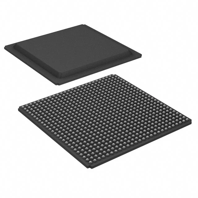
사양
Part Number Explanation
This is an AMD Xilinx Kintex UltraScale+ FPGA built on 16nm FinFET process, featuring integrated UltraRAM for large on-chip storage, oriented toward commercial high-speed data processing and low-latency embedded systems.
- XCKU3P: Entry-level model of Kintex UltraScale+ P-series, equipped with dedicated UltraRAM memory blocks
- -2: Speed Grade 2, balanced performance tier, striking a compromise between maximum operating frequency and power consumption
- FFVB676: 676-ball flip-chip FCBGA compact package
- C: Commercial temperature grade, junction temperature operating range: 0°C ~ +85°C
On-Chip Hardware Resources
Logic & DSP Computing Units
- Total Logic Cells: 221,280
- DSP48E2 arithmetic slices: 1128 units
Applied for FFT computation, digital filtering, intermediate wireless baseband processing, image algorithm acceleration and medium-scale matrix calculations
내장 메모리 리소스
- Total Block RAM: 14.5 Mb
- UltraRAM dedicated memory: 13.5 Mb, ideal for video frame buffers, deep packet buffering and large algorithm temporary storage
- LUT-based distributed RAM for ultra-low latency small-capacity cache
클럭 관리 모듈
Multiple MMCM and PLL clock management tiles are integrated on the chip. They support clock multiplication, division, arbitrary phase shifting and jitter reduction to fulfill timing demands of multi-clock high-speed digital systems.
High-Speed Transceivers & General I/O
- 8-channel GTH serial transceivers, maximum single-lane rate up to 16.375 Gbps
Supported protocols: PCIe Gen3, 10G Ethernet, JESD204B/C, Aurora
- Available user I/O pins: 280
Contains HR wide-voltage I/O banks and HP high-performance I/O banks, compatible with LVCMOS, LVDS, HSTL, SSTL and all mainstream differential signal standards
- Built-in SYSMON monitor: Real-time detection of die temperature, internal power supply voltages and external analog input signals
전원 공급 장치 사양
Nominal core logic voltage: 0.85 V
Separate independent power domains are allocated for core logic, memory arrays, transceivers and I/O interfaces. Dynamic voltage and frequency adjustment can be activated to lower power draw under light workloads.
Typical total power consumption: 10W ~ 30W, passive heat sinks suffice for compact commercial embedded hardware
포장 및 SMT 조립 요건
- Package: 676-pin flip-chip FCBGA ball grid array
- Moisture Sensitivity Level: MSL3; all reflow soldering shall be finished within 168 hours once vacuum packaging is opened
- Lead-free construction, fully RoHS compliant
- Supplied in anti-static trays for automated industrial PCB mass production
Environmental and Reliability Features
Designed for stable operation in indoor constant-temperature commercial environments only, not suitable for outdoor extreme low/high temperature industrial scenarios.
It supports 256-bit AES bitstream encryption for design IP protection, SEU radiation error correction and partial dynamic reconfiguration, delivering reliable performance for commercial vision devices, indoor communication equipment and desktop data acquisition systems.
일반적인 애플리케이션 시나리오
- Indoor small cell base station baseband processing boards and compact network gateway modules
- Desktop multi-channel machine vision inspection equipment and industrial camera image processing units
- Bench-top oscilloscopes, signal analyzers and laboratory precision measurement instruments
- Desktop high-speed PCIe data acquisition and storage accelerator cards
- Commercial multi-screen video splicing and real-time video processing terminals
- Algorithm verification prototype boards and custom embedded commercial SOM core modules


