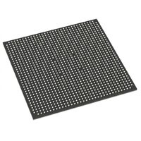
| 모델 P/N | 시리즈 | 실험실/CLBS 수 | 속도 등급 | 논리 요소/셀 수 | 총 램 비트 | I/O 수 | 전압 - 공급 | 마운팅 유형 | 작동 온도 | 패키지 / 케이스 | 공급업체 디바이스 패키지 |
|---|---|---|---|---|---|---|---|---|---|---|---|
| XC4VLX100-10FFG1148I | Virtex-4 LX | 11.520,00 | -10,00 | 99840 | 4478976 | 768 | 1.14V ~ 1.26V | 표면 실장 | -40 °C ~ +100 °C (Industrial) | 1148-BBGA (FCBGA) | 1148-FCBGA |
XC4VLX100-10FFG1148I: High-Density Industrial FPGA for Robust System Logic
그리고 XC4VLX100-10FFG1148I is a high-performance, industrial-grade FPGA member of the Xilinx Virtex®-4 LX family. Built on the innovative 90nm ASMBL™ (Advanced Silicon Modular Block) architecture, this device is specifically engineered for designers who require a massive logic fabric—110,592 Logic Cells—without moving to the extreme power envelopes of the LX160 or LX200 variants.
Housed in the FFG1148 Lead-Free Flip-Chip BGA package, this device is binned for Industrial-grade (-40°C to +100°C) operation, ensuring timing stability and long-term reliability in the most demanding environmental conditions.
Core Engineering Highlights
Logic Capacity & Scalability: With 110,592 Logic Cells and over 12,000 CLBs, the LX100 provides the “headroom” necessary to consolidate multiple IP cores, custom state machines, and high-speed protocol bridges into a single chip.
Industrial Thermal Resilience: 그리고 “-I” rating ensures that the FPGA maintains its -10 speed grade timing characteristics across a wide temperature spectrum. This is a critical requirement for outdoor telecommunications infrastructure and ruggedized industrial automation.
Massive I/O Density: 그리고 FFG1148 package exposes 768 User I/Os. Leveraging Xilinx’s SelectIO™ technology, it supports an extensive array of differential (LVDS) and single-ended (HSTL/SSTL) signaling standards, ideal for interfacing with high-width DDR2 or QDR memory banks.
Dedicated DSP Power: Integrated with 96 DSP48 slices. These hard-coded blocks facilitate high-speed 18×18 arithmetic and MAC operations, enabling real-time signal processing and filtering without exhausting general logic fabric.
Optimized Memory Hierarchy: 특징 4,320 Kb of Block RAM (BRAM), providing the low-latency buffering and deep FIFO structures required for high-throughput data streams.
Technical Specification Matrix
| 기능 | 사양 |
| 논리 셀 | 110,592 |
| Total Block RAM | 4,320 Kb |
| DSP48 Slices | 96 |
| User I/Os | 768 |
| 속도 등급 | -10 |
| 작동 온도 | Industrial (-40°C to +100°C Tj) |
| 패키지 | FFG1148 (Lead-Free / 1.0mm Pitch) |
| 코어 전압 | 1.2V |
Why Specify the LX100-10I?
1. Predictable Timing Closure
The ASMBL architecture interleaves logic, memory, and DSP columns, which significantly reduces routing congestion. For engineers working on designs with >80% logic utilization, the LX100-10I offers much more predictable timing closure compared to less advanced architectures.
2. Superior Signal Integrity
그리고 FFG1148 Flip-Chip package is specifically designed to minimize parasitic inductance. The dense grid of power and ground pins helps suppress Simultaneous Switching Noise (SSN), which is vital for maintaining robust noise margins in high-speed parallel bus designs.
3. Long-Lifecycle Stability
The Virtex-4 series remains a cornerstone for high-reliability systems with 10–15 year service requirements. Choosing the LX100-10I provides a proven, well-documented platform with a stable toolchain, reducing the risk of mid-lifecycle architectural bugs.
Primary Applications
산업 제어: Multi-axis robotics and high-precision motor control.
Telecommunications: Base station signal processing and localized switching.
Medical Equipment: Real-time data acquisition for CT/MRI reconstruction backends.
Defense & Aerospace: Ground support systems and secure communication bridges.


