






| MODEL P / N | SERI | JUMLAH LABORATORIUM/CLBS | TINGKAT KECEPATAN | JUMLAH ELEMEN / SEL LOGIKA | TOTAL BIT RAM | JUMLAH I / O | TEGANGAN - PASOKAN | JENIS PEMASANGAN | SUHU PENGOPERASIAN | PAKET / KASUS | PAKET PERANGKAT PEMASOK |
|---|---|---|---|---|---|---|---|---|---|---|---|
| XCKU095-1FFVA1156E | Kintex UltraScale | 67,20 | -1,00 | 1.176.000 LE | ~ 60,52 Mbit | 520 | VCCINT ~ 0,92 V | Pemasangan di permukaan (FCBGA) | 0 °C hingga +100 °C | FCBGA-1156 | 1156-FCBGA |
XCKU095-1FFVA1156E
Produsen: Xilinx
Sel Logika: 1,143,360
Irisan Logika: 178,650
RAM tertanam (eRAM): 48,960 Kb (1,360 × 36Kb Block RAM)
I/O Pengguna Maksimum: 500
Paket: FFVA1156 (Flip-Chip BGA)
Tingkat Kecepatan: -1
Suhu Pengoperasian: Diperpanjang (0°C hingga +100°C)
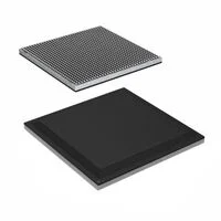
Spesifikasi
Rincian Nomor Bagian
This is AMD Xilinx Kintex UltraScale series high-performance FPGA built on 20nm UltraScale process, optimized for high-throughput data processing, wireless baseband, network acceleration and multi-channel high-speed serial transmission applications.
- XCKU095: Large-capacity flagship model of Kintex UltraScale family
- -1: Speed Grade 1, baseline timing grade, cost-optimized for non-extreme high-frequency design scenarios
- FFVA1156: 1156-ball flip-chip FCBGA surface-mount package
- E: Extended commercial temperature grade, junction temperature operating range: 0°C ~ +100°C
Sumber Daya Perangkat Keras Inti pada Chip
Logic & DSP Computing Resources
- Total Logic Cells: 1,176,000
- Total Look-Up Tables (LUTs): 537,600
- Total Flip-Flops: 1,075,200
- DSP48E2 arithmetic slices: 2,760 units
For massive FFT, digital filtering, 5G/4G wireless baseband processing, matrix computation, AI lightweight inference and high-throughput signal arithmetic operations
Sumber Daya Memori Terintegrasi
- Total Block RAM capacity: 59.1 Mbit
Consists of independent 36K dual-port RAM blocks for large data buffering, FIFO queues and algorithm intermediate storage; LUT-based distributed RAM supports ultra-low latency tiny cache
Clock Management Subsystem
Multiple MMCM + PLL clock management tiles integrated on chip, supporting clock multiplication/division, arbitrary phase adjustment, jitter filtering and multi-clock domain generation, adapting to ultra-high-speed synchronous digital system timing requirements
Transceiver Serial Berkecepatan Tinggi & I/O Umum
- 20-channel GTH high-speed differential transceivers, maximum single-lane rate up to 16.375 Gbps
Supported protocols: PCIe Gen3, 10G Ethernet, Aurora, JESD204B/C, Interlaken, fiber optical transmission
- Total available user configurable I/O pins: 520
Includes HP high-performance I/O banks and HR high-range voltage I/O banks; supports LVCMOS, LVDS, differential HSTL/SSTL and all mainstream industrial signal standards; configurable I/O voltage from 1.2V to 3.3V
- Built-in SYSMON system monitoring module: real-time monitoring of chip internal temperature, multi-group power supply voltages and external analog input signals
Spesifikasi Catu Daya
- Nominal core logic voltage (VCCINT): 0.92V ~ 0.98V
Independent power domains configured for core logic, block RAM, transceivers and I/O banks; dynamic voltage/frequency scaling is supported to reduce power consumption under light load
Typical full-load overall power consumption: 70W ~ 130W, forced air cooling or liquid cooling is required for continuous stable operation
Persyaratan Pengemasan & Perakitan SMT
- Package: 1156-pin flip-chip FCBGA ball grid array
- Moisture Sensitivity Level: MSL3; all reflow soldering procedures must be completed within 168 hours after vacuum packaging is opened
- Fully lead-free construction, compliant with global RoHS environmental directives
- Packaged in anti-static trays for automated industrial PCB mass production
Karakteristik Lingkungan & Keandalan
Only extended commercial temperature specification, suitable for indoor industrial equipment, communication room and stable ambient environments, not applicable to outdoor low-temperature extreme working conditions.
Supports 256-bit AES bitstream encryption for IP protection, SEU single-event upset radiation error correction, partial dynamic reconfiguration and integrated PCIe hard macro, with excellent long-term operational stability
Skenario Aplikasi Umum
- Wireless communication equipment: 4G/5G macro station & small cell baseband processing boards, radio remote unit signal processing modules
- Network & storage acceleration: data center smart NIC, storage array controller, 100G Ethernet switching and gateway hardware
- High-end industrial machine vision: multi-camera synchronous image processing, medical imaging reconstruction and backhaul equipment
- High-precision test instruments: multi-channel oscilloscopes, spectrum analyzers and ultra-high-speed data acquisition cards
- Radar signal processing, aerospace onboard data forwarding and high-speed parallel computing acceleration platforms
- Custom FPGA acceleration boards for algorithm verification and prototype development


