






| MODEL P / N | SERI | JUMLAH LABORATORIUM/CLBS | TINGKAT KECEPATAN | JUMLAH ELEMEN / SEL LOGIKA | TOTAL BIT RAM | JUMLAH I / O | TEGANGAN - PASOKAN | JENIS PEMASANGAN | SUHU PENGOPERASIAN | PAKET / KASUS | PAKET PERANGKAT PEMASOK |
|---|---|---|---|---|---|---|---|---|---|---|---|
| XC7Z035-L2FFG676E | Zynq-7000 SoC | 42,98 | 0,00 | 275.000 LE | 17600000 | 0 | 1.0 V | SMD / SMM | Diperpanjang (0 ° C ... 100 ° C) | FCBGA-676 | FCBGA-676 |
XC7Z035-L2FFG676E
Produsen: Xilinx
Sel Logika: ~28.000 (Versi Daya Rendah)
RAM tertanam (eRAM): ~1,0 Mb
Hitungan I/O: ~676 pin
Paket: FFG?676
Suhu Pengoperasian: Komersial (0°C hingga +85°C)
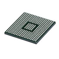
Spesifikasi
Rincian Nomor Bagian
This is Xilinx Zynq-7000 AP SoC built on 28nm process, combining dual-core Cortex-A9 processing system and large-scale Artix-7 programmable logic, optimized for low-power wide-temperature embedded industrial applications.
- XC7Z035: High-end large logic capacity model of Zynq-7000 family
- L2: Low-power speed grade 2, supports reduced core voltage operation to cut static and dynamic power consumption while retaining moderate timing performance
- FFG676: 676-ball flip-chip FCBGA compact package
- E: Kelas suhu industri yang diperluas, rentang suhu sambungan: -40°C ~ +125°C
On-Chip Complete Hardware Architecture
1. Processing System (PS: ARM Subsystem)
- Dual-core ARM Cortex-A9 MPCore, maximum clock speed up to 1000MHz
- Each core has 32KB I-cache + 32KB D-cache; 512KB shared L2 cache
- Integrated NEON floating-point & SIMD engine for multimedia, signal computation acceleration
- Standard onboard peripherals: Dual Gigabit Ethernet, USB2.0 OTG, SD/MMC, CAN, UART, SPI, I2C, GPIO
- Secure boot supported for system startup security protection
2. Programmable Logic (PL: Artix-7 FPGA Fabric)
- Jumlah Sel Logika: 277.760
- DSP48E1 arithmetic blocks: 900 units, used for digital filtering, FFT, multi-channel image processing and matrix calculation
- Total Block RAM: 17.0 Mb
- Multiple MMCM+PLL clock management tiles for multi-clock generation and jitter suppression
- Tidak terdapat transceiver serial berkecepatan tinggi yang terintegrasi
3. I/O & Analog Monitoring Module
- Available user I/O pins: 360
- Configurable I/O bank voltage 1.2V~3.3V, compatible with LVCMOS, LVDS and mainstream differential signal standards
- On-chip dual-channel 12-bit XADC: real-time monitoring of die temperature, internal supply voltages and external analog signals
Spesifikasi Catu Daya
Tegangan inti standar: 1,0 V
Low-power mode core voltage can be lowered to reduce power draw under light workloads
Separate power domains for PS and PL sections
Typical total power consumption: 9W ~ 28W; passive heat sinks work for compact low-power embedded devices
Persyaratan Pengemasan & Perakitan SMT
- Package: 676-pin FCBGA flip-chip ball grid array
- Moisture Sensitivity Level: MSL3; reflow soldering must be completed within 168 hours after vacuum bag opening
- Lead-free construction, RoHS compliant
- Supplied in anti-static trays for automated PCB mass production
Reliability & Environmental Performance
Stable continuous operation under extreme temperature swings and strong electromagnetic interference industrial environments.
Supports bitstream encryption and SEU error checking, designed for outdoor industrial equipment, vehicle-mounted systems and airborne lightweight electronic devices requiring wide temperature adaptability.
Skenario Aplikasi Umum
- Outdoor industrial motion controllers, field equipment edge control gateways
- Rugged portable machine vision inspection terminals for field operation
- Vehicle-mounted multi-channel data recording and automotive perception preprocessing units
- Handheld high-precision measuring instruments and vibration monitoring acquisition equipment
- Miniature airborne signal preprocessing and short-range radar peripheral control boards
- Wide-temperature industrial SOM core modules and rugged embedded secondary development platforms


