






| Referencia | Fabricante | Familia FPGA | Elementos lógicos (LE) | Memoria integrada | DSP / Multiplicadores | Número máximo de E/S | Tensión del núcleo | Tensión de E/S | Temperatura de funcionamiento | Paquete | Nodo de proceso | Frecuencia máxima típica | Aplicaciones de destino | RoHS |
| EP2C5T144C8N | ALTERA | Cyclone® II | ~5,120 | ~119 Kbits | Limitado | Hasta el 89 | ~1.2 V | Hasta 3,3 V | 0 °C a +85 °C | TQFP-144 | 90 nm | ~250 MHz | Sistemas heredados, control lógico simple | Sí |
EP2C5T144C8N
Fabricante: Altera (Intel)
Células lógicas: 4,608 Logic Elements (LEs)
Rebanadas lógicas: Logic Array Blocks (LABs)
RAM integrada (eRAM): 119 Kbits embedded memory
Paquete: TQFP-144
Temperatura de funcionamiento: Uso comercial (0 °C a +85 °C)
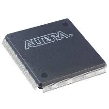
Especificaciones
EP2C5T144C8N is a cost-effective Intel (Altera) Cyclone II commercial-grade FPGA built with TSMC 90nm low-k process, balancing moderate logic density, embedded memory and multipliers for low-to-medium complexity digital logic, signal processing and embedded control systems.
👉 It’s not a high-density high-end FPGA for massive parallel computing or multi-gigabit serial interfaces.
👉 It’s an economical general-purpose programmable logic chip for cost-sensitive embedded, industrial control and educational development hardware.
Key Features of EP2C5T144C8N FPGA
Digital design engineers and equipment developers select EP2C5T144C8N for its balanced performance, compact packaging and affordable overall BOM cost:
- Total 4,608 logic elements (LEs) distributed across 288 Logic Array Blocks (LABs) for medium-scale digital circuit implementation
- On-chip embedded block RAM with total 119,808 RAM bits for data buffering and FIFO cache design
- 13 built-in 18×18-bit embedded hardware multipliers to accelerate filtering, PID control and simple DSP algorithms
- Dual independent PLL clock management modules, supporting max 320MHz internal clock frequency for timing optimization
- -8 commercial speed grade with stable timing closure for standard frequency operation scenarios
- 144-pin TQFP surface mount package (20×20mm), bringing out 89 usable user I/O pins for peripheral connection
- Core supply voltage range 1.15V–1.25V, compatible with 3.3V LVTTL I/O voltage standard
- Multiple configuration modes supported: Active Serial, Passive Serial and JTAG for flexible firmware download and debugging
- Native support for Nios II soft-core embedded processor to realize custom single-chip SoC architecture
- Commercial operating temperature range: 0°C to +85°C junction temperature
- MSL 3 moisture sensitivity rating, RoHS-compliant lead-free packaging for mass SMT production
- Low power consumption compared to peer 90nm FPGA devices, suitable for fanless compact equipment
- Stable long-lifecycle supply support for legacy equipment maintenance and small-batch industrial projects
Aplicaciones típicas
FPGA development boards, university electronic teaching and training platforms
Small industrial PLC auxiliary control modules and sensor signal acquisition boards
Low-speed serial communication protocol conversion equipment
Motor PID motion control and stepper motor drive logic circuits
Audio signal filtering, simple image pre-processing and low-rate data processing
Medical portable testing instrument digital logic control units
Consumer smart equipment interface expansion and peripheral logic bridging
Test & measurement small signal conditioning and timing generator hardware
Low-cost digital display drive and LED matrix control systems
LXB Semicon supplies original EP2C5T144C8N FPGA


