






| МОДЕЛЬ П/Н | СЕРИИ | КОЛИЧЕСТВО ЛАБОРАТОРИЙ/КЛБ | УРОВЕНЬ СКОРОСТИ | КОЛИЧЕСТВО ЛОГИЧЕСКИХ ЭЛЕМЕНТОВ / ЯЧЕЕК | ВСЕГО БИТОВ ОЗУ | КОЛИЧЕСТВО ВХОДОВ/ВЫХОДОВ | НАПРЯЖЕНИЕ - ПИТАНИЕ | ТИП КРЕПЛЕНИЯ | РАБОЧАЯ ТЕМПЕРАТУРА | УПАКОВКА / КЕЙС | УПАКОВКА УСТРОЙСТВА ПОСТАВЩИКА |
|---|---|---|---|---|---|---|---|---|---|---|---|
| XC7Z100-2FFG900C | Zynq-7000 | 26.150,00 | -2,00 | 277,400 | 26200000 | 250 | 1.0 V | Монтаж на поверхность | Коммерческий (0 °C ~ 85 °C) | BGA-900 | 900-FCBGA (31×31 мм) |
XC7Z100-2FFG900C
Производитель: Xilinx
Логические ячейки: 444,000
Логические срезы: 69,000
Встроенная оперативная память (eRAM): 26,280 Kb (730 × 36Kb Block RAM)
Максимальный пользовательский ввод/вывод: 300
Упаковка: FFG900 (Flip-Chip BGA)
Класс скорости: -2
Рабочая температура: Коммерческий (от 0°C до +85°C)
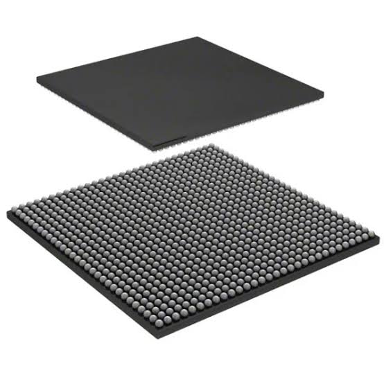
Технические характеристики
Part Number Overview
This high-performance commercial heterogeneous all-programmable SoC is developed by Xilinx under the Zynq-7000 product portfolio, manufactured with 28nm semiconductor process. It combines dual-core ARM Cortex-A9 processing unit and full-capacity Kintex-7 flagship FPGA resources, tailored for high-throughput signal processing, multi-channel video processing and high-speed data transmission devices running under steady indoor ambient temperature.
- XC7Z100: Top flagship variant of Zynq-7000 series, equipped with the maximum amount of Kintex-7 programmable logic resources
- -2: Speed Grade 2, standard balanced performance grade. It reserves sufficient timing margin for most complex high-frequency logic designs, achieving a good balance between maximum operating frequency, timing stability and power consumption
- FFG900: 900-ball flip-chip FCBGA package, dimension 31mm × 31mm. Compact size supports miniaturized hardware layout compared to the 1156-ball package version
- C: Commercial temperature range, junction temperature operating scope: 0°C ~ +85°C
Full On-Chip Hardware Architecture
1. Processing System (PS Section)
- Dual-core ARM Cortex-A9 MPCore processor, maximum operating frequency up to 1000MHz
- Each core has dedicated 32KB instruction L1 cache and 32KB data L1 cache, paired with shared 1MB L2 cache
- Built-in NEON SIMD floating-point arithmetic unit, which accelerates digital signal algorithms and audio & video encoding/decoding workloads efficiently
- 256KB on-chip OCM memory integrated; supports external DDR2 and DDR3 memory expansion
- Complete peripheral interfaces: Dual Gigabit Ethernet, USB 2.0 OTG, SD/MMC controller, dual CAN 2.0B, UART, SPI, I2C and general-purpose MIO GPIO
- 256-bit AES secure boot together with SHA-256 checksum verification is available to prevent firmware tampering and secure embedded system operation
2. Programmable Logic (PL Section, Kintex-7 Architecture)
- Total Logic Cells: 444000
- DSP48E1 arithmetic blocks: 2020 units, suited for large-scale FFT calculation, digital filtering, wireless baseband processing, multi-channel 4K video algorithm acceleration and large matrix computation
- Total Block RAM Capacity: 26.5Mb
- Multiple MMCM and PLL clock modules for multi-domain clock generation and high-frequency clock jitter reduction
- 16 GTX high-speed serial transceivers, maximum transmission rate 12.5Gbps, compatible with PCIe Gen2, 10G Ethernet, CPRI, JESD204B, Aurora serial protocols
3. I/O Resources & On-Chip Monitoring Module
- Available configurable user I/O pins: 362
- Adjustable I/O bank voltage ranging from 1.2V to 3.3V, compatible with LVCMOS, LVDS, HSTL, SSTL and mainstream differential signal standards
- Dual-channel 12-bit XADC module on chip: Real-time monitoring of die junction temperature, internal power supply voltages and external analog input signals
Power Specifications
Nominal core operating voltage: 1.0V
PS and PL domains adopt independent isolated power supply designs
Typical overall power consumption: 16W ~ 39W. Active cooling heatsink is required for continuous full-load stable operation
Packaging & SMT Requirements
- Package Type: 900-pin FCBGA flip-chip ball grid array
- Moisture Sensitivity Level: MSL4. Reflow soldering must be finished within 72 hours after vacuum packaging is opened
- Lead-free design, fully compliant with RoHS environmental regulations
- Packed in anti-static trays for automated PCB mass production
Environmental Performance & Reliability
This chip is designed exclusively for constant-temperature indoor environments such as laboratories and equipment rooms, not applicable to outdoor industrial scenes with severe temperature fluctuation and strong electromagnetic interference.
It supports bitstream AES encryption and SEU error detection, delivering stable long-term operation for high-end test instruments, embedded video servers and software-defined radio devices.
Основные области применения
- Laboratory-grade software-defined radio baseband platforms, wireless communication testing instruments
- Multi-channel 4K video encoding, decoding and intelligent surveillance analysis terminals
- High-end oscilloscopes, spectrum analyzers and high-speed multi-channel data recorders
- Data center edge gateway and storage acceleration control modules
- Medical image reconstruction and diagnostic device main control boards
- High-performance embedded SOM modules and complex algorithm prototype verification platforms


