






| 모델 P/N | 시리즈 | 실험실/CLBS 수 | 속도 등급 | 논리 요소/셀 수 | 총 램 비트 | I/O 수 | 전압 - 공급 | 마운팅 유형 | 작동 온도 | 패키지 / 케이스 | 공급업체 디바이스 패키지 |
|---|---|---|---|---|---|---|---|---|---|---|---|
| XCKU3P-3FFVB676E | 킨텍스® 울트라스케일+ | 20,34 | -3,00 | 355,950 LE | 31,641,600비트 | 0 | ~0.85 V | 표면 실장 | 0°C - 100°C | FCBGA-676 | 676-FCBGA(27×27) |
사양
부품 번호 분석
This is AMD Xilinx Kintex UltraScale+ family low-power FPGA fabricated on 16nm FinFET process, designed for embedded signal processing, portable instruments and extreme temperature industrial devices.
- XCKU3P: Entry-level member of Kintex UltraScale+ P-series with built-in UltraRAM on-chip large memory
- -3: Speed Grade 3, power-optimized grade, prioritizes power efficiency over maximum operating frequency
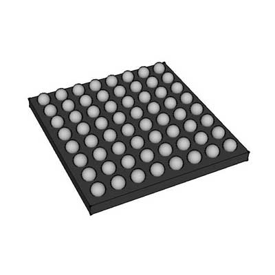
- FFVB676: 676-ball flip-chip FCBGA compact package
- E: Extended industrial temperature grade, junction temperature operating range: -40°C ~ +125°C
On-Chip Hardware Resources
Logic and DSP Resources
- Total Logic Cells: 221280
- DSP48E2 dedicated arithmetic blocks: 1128 units
Used for digital filtering, FFT calculation, sensor data processing, lightweight image algorithms and small-scale matrix operations
임베디드 메모리
- Total Block RAM: 14.5 Mb
- On-chip UltraRAM: 13.5 Mb, suitable for image frame buffering, deep data caching and large algorithm intermediate storage
- LUT-based distributed RAM for ultra-low latency temporary data storage
Clock Management System
Multiple MMCM and PLL clock management tiles are integrated. It supports clock frequency multiplication/division, arbitrary phase adjustment and jitter attenuation to meet timing requirements of multi-clock digital systems
High-Speed Transceivers & I/O Interfaces
- 8 GTH high-speed serial transceivers, maximum single lane rate up to 16.375 Gbps
Supported protocols: PCIe Gen3, 10G Ethernet, JESD204B/C, Aurora
- Available user I/O pins: 280
Equipped with HR wide-voltage I/O banks and HP high-speed I/O banks, compatible with LVCMOS, LVDS, HSTL, SSTL and mainstream differential signal standards
- Built-in SYSMON module: Real-time monitoring of chip internal temperature, power supply voltages and external analog input signals
전원 공급 장치 사양
Nominal core operating voltage: 0.85 V
Independent power domains are configured for core logic, memory modules, transceivers and I/O interfaces. Dynamic voltage and frequency scaling can be enabled to reduce power consumption under light loads.
Typical overall power consumption: 8W ~ 27W, passive heat dissipation is applicable for miniature compact embedded devices
Packaging and Assembly Requirements
- Package: 676-pin flip-chip FCBGA ball grid array
- Moisture Sensitivity Level: MSL3; reflow soldering must be completed within 168 hours after opening vacuum packaging
- Lead-free design, fully compliant with RoHS environmental standards
- Packaged in anti-static trays for automated industrial PCB mass production
Reliability & Environmental Performance
It can run stably for a long time under extreme temperature changes and strong electromagnetic interference environments.
Supports 256-bit AES bitstream encryption for IP protection, SEU single-event upset error correction and partial dynamic reconfiguration, meeting the high stability requirements of automotive electronics, outdoor industrial equipment and portable airborne terminals.
일반적인 애플리케이션 시나리오
- Handheld software-defined radio, miniature wireless baseband signal preprocessing modules
- Portable multi-channel data recorders, vibration monitoring terminals and handheld precision measuring instruments
- Miniature short-range radar front-end signal acquisition and echo processing boards
- Vehicle-mounted video preprocessing units and automotive peripheral control modules
- Field portable industrial visual inspection equipment
- Low-power PCIe data acquisition cards and custom embedded core carrier boards


