






| 모델 P/N | 시리즈 | 실험실/CLBS 수 | 속도 등급 | 논리 요소/셀 수 | 총 램 비트 | I/O 수 | 전압 - 공급 | 마운팅 유형 | 작동 온도 | 패키지 / 케이스 | 공급업체 디바이스 패키지 |
|---|---|---|---|---|---|---|---|---|---|---|---|
| XC7Z045-2FBG676C | Zynq-7000 SoC | 27,33 | -2,00 | ~350,000 LE | 19200000 | 250 | 1.0 V | SMD/SMT | 상업용(0°C ~ 85°C) | FCBGA-676 | FCBGA-676 |
사양
부품 번호 정의
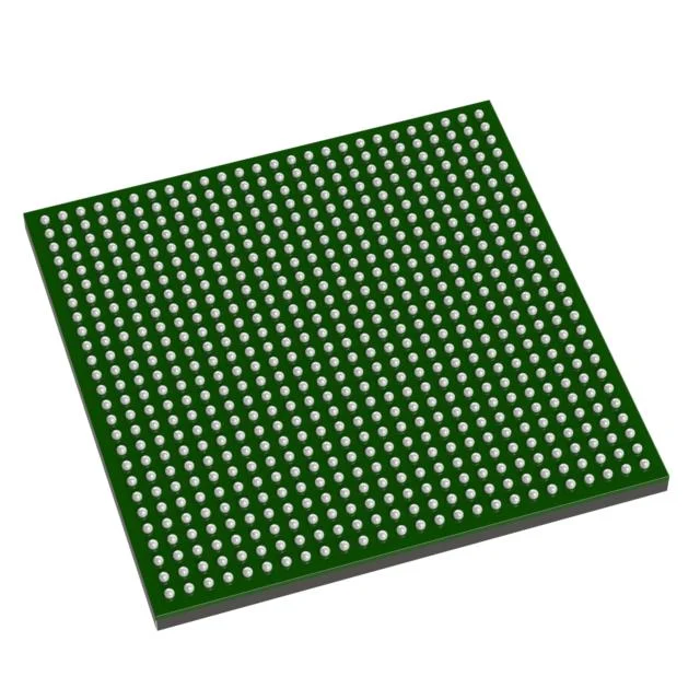
This is Xilinx Zynq-7000 high-performance heterogeneous SoC manufactured on the 28nm process node. It integrates dual-core ARM Cortex-A9 processing subsystem and Kintex-7 grade large-capacity FPGA logic resources, designed for commercial high-speed embedded computing, multi-channel image processing and high-bandwidth data acquisition applications.
- XC7Z045: Flagship high-density model of Zynq-7000 series, equipped with Kintex-class programmable logic resources
- -2: Speed Grade 2, mainstream high-speed timing grade with sufficient timing margin for high-frequency logic design
- FBG676: 676-ball flip-chip FCBGA compact package
- C: Commercial temperature grade, junction temperature operating range: 0°C ~ +85°C
Complete On-Chip Hardware Architecture
1. Processing System (PS: ARM Domain)
- Dual-core ARM Cortex-A9 MPCore, maximum operating frequency up to 1000 MHz
- Each core is configured with 32KB instruction cache and 32KB data cache; 1MB shared L2 cache
- Built-in NEON SIMD floating-point acceleration engine for multimedia decoding, digital signal algorithm acceleration
- Abundant standard peripherals: Dual Gigabit Ethernet, USB 2.0 OTG, SD/MMC interface, CAN bus, UART, SPI, I2C, general-purpose GPIO
- Secure boot function is supported to protect system firmware from tampering
2. Programmable Logic (PL: Kintex-7 FPGA Fabric)
- Total Logic Cells: 354,560
- DSP48E1 arithmetic blocks: 1920 units, applied for large-scale FFT computation, digital filtering, wireless baseband preprocessing, multi-channel image algorithm acceleration and matrix operations
- Total Block RAM: 19.2 Mb
- Multiple MMCM and PLL clock management modules to generate multi-group clocks and suppress clock jitter
- No embedded high-speed serial transceivers inside the chip
3. I/O Resources & On-Chip Monitoring Module
- Available user configurable I/O pins: 360
- I/O banks support adjustable voltage from 1.2V to 3.3V, compatible with LVCMOS, LVDS, HSTL and other mainstream differential signal standards
- Integrated dual-channel 12-bit XADC analog monitor: Real-time acquisition of chip internal temperature, power supply voltages and external analog input signals
전원 공급 장치 사양
Nominal core logic voltage: 1.0 V
Independent power domains are allocated for PS processing system and PL programmable logic respectively
Typical overall power consumption: 13W ~ 34W, a heat sink is required for continuous full-load operation
포장 및 SMT 조립 요건
- Package: 676-pin flip-chip FCBGA ball grid array
- Moisture Sensitivity Level: MSL3; all reflow soldering must be completed within 168 hours after vacuum packaging is unsealed
- Lead-free structure, fully compliant with RoHS environmental directives
- Supplied in anti-static trays for automated PCB mass production
Environmental and Reliability Characteristics
Only suitable for stable indoor commercial and laboratory environments, cannot adapt to outdoor extreme high/low temperature industrial scenarios.
It supports bitstream encryption protection and SEU single-event upset detection, delivering stable long-term operation for indoor industrial automation equipment, commercial vision inspection systems and desktop precision test instruments.
일반적인 애플리케이션 시나리오
- High-precision multi-axis motion controllers, centralized control units for automated production lines
- Multi-camera synchronous industrial machine vision platforms, high-speed image capture and processing terminals
- Multi-channel high-speed data recorders, vibration signal analysis and monitoring instruments
- Indoor medical diagnostic equipment main control boards and medical image preprocessing modules
- Intelligent surveillance multi-channel video decoding and edge analysis nodes
- High-performance embedded core boards and algorithm prototype verification platforms for secondary development


