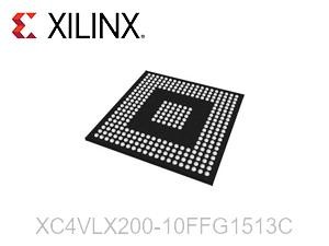
| 모델 P/N | 시리즈 | 실험실/CLBS 수 | 속도 등급 | 논리 요소/셀 수 | 총 램 비트 | I/O 수 | 전압 - 공급 | 마운팅 유형 | 작동 온도 | 패키지 / 케이스 | 공급업체 디바이스 패키지 |
|---|---|---|---|---|---|---|---|---|---|---|---|
| XC4VLX200-10FFG1513C | Virtex-4 LX | 22.272,00 | -10,00 | 200448 | 6193152 | 960 | 1.14V ~ 1.26V | 표면 실장 | 0°C ~ +85°C(상업용) | 1513-BBGA (FCBGA) | 1513-FCBGA |
XC4VLX200-10FFG1513C: The Ultimate Logic Density for Large-Scale System Integration
그리고 XC4VLX200-10FFG1513C is the flagship high-capacity FPGA within Xilinx’s Virtex®-4 LX family. It is engineered for hardware architects who require massive programmable logic resources without moving to multi-chip partitions. Built on the 90nm ASMBL™ (Advanced Silicon Modular Block) architecture, the LX200 provides a staggering 200,448 Logic Cells, making it the definitive choice for high-end commercial applications such as ASIC prototyping, medical imaging, and complex network switching fabrics.
This Commercial-grade (0°C to +85°C) device, featuring the -10 speed grade, offers the industry’s most balanced logic-to-cost ratio for high-gate-count designs.
Engineering Core Highlights
Maximum Logic Capacity: With over 200k logic cells, the LX200 allows for the consolidation of entire system-on-chip (SoC) designs, including multiple MicroBlaze™ processors and extensive custom RTL, into a single device.
Industry-Leading I/O Count: Housed in the FFG1513 package, this FPGA breaks out 960 User I/Os. This massive I/O density is critical for interfacing with wide parallel buses, dual-bank DDR2 memory, and high-width backplanes.
Deep Memory Resources: 특징 6,048 Kb of Block RAM, providing the necessary bandwidth for deep FIFO buffering and high-resolution video frame storage, minimizing the need for external SRAM.
Dedicated DSP Power: Integrated with 96 XtremeDSP™ slices, capable of handling arithmetic-intensive tasks like 3D image reconstruction and complex digital filtering at high clock frequencies.
Signal & Power Integrity: 그리고 FFG1513 Flip-Chip BGA package is designed with a dense grid of power and ground pins to minimize Simultaneous Switching Noise (SSN), ensuring clean signal eyes even under high toggle rates.
Technical Specification Matrix
| 기능 | 사양 |
| 논리 셀 | 200,448 |
| Configurable Logic Blocks (CLBs) | 22,512 |
| Total Block RAM | 6,048 Kb |
| DSP48 Slices | 96 |
| Maximum User I/O | 960 |
| 속도 등급 | -10 (Standard Performance) |
| 패키지 | FFG1513 (Lead-Free Flip-Chip BGA) |
| 작동 온도 | 상업용(0°C ~ +85°C) |
The Hardware Architect’s Perspective: Why Specify the LX200-10C?
1. Eliminating Multi-Chip Latency
In large-scale designs, partitioning logic across two smaller FPGAs introduces significant timing penalties due to chip-to-chip interconnects. The LX200 allows you to keep your entire critical path on a single die, drastically simplifying timing closure and PCB routing.
2. Robust Thermal Management
Despite its massive logic count, the FFG (Lead-Free) Flip-Chip package provides excellent thermal conductivity. This allows for direct-contact cooling solutions, ensuring the device remains stable even when logic utilization approaches 90%.
3. Long-Term Reliability and Toolchain Maturity
The Virtex-4 LX200 is a mature, proven platform. Its timing models are rock-solid, and the development ecosystem is highly stable, making it a “low-risk” choice for high-value commercial systems that require a 10+ year deployment lifecycle.
Primary Applications
High-Performance Computing: Hardware acceleration for financial modeling and genomic research.
Broadcasting & Pro-AV: 4K/8K real-time video processing and format conversion.
Medical Systems: High-speed data acquisition for CT/MRI scanners.
ASIC/SoC Prototyping: Large-scale logic verification and emulation.


