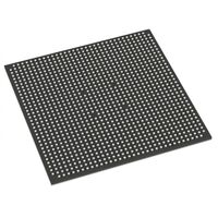
| 모델 P/N | 시리즈 | 실험실/CLBS 수 | 속도 등급 | 논리 요소/셀 수 | 총 램 비트 | I/O 수 | 전압 - 공급 | 마운팅 유형 | 작동 온도 | 패키지 / 케이스 | 공급업체 디바이스 패키지 |
|---|---|---|---|---|---|---|---|---|---|---|---|
| XC4VLX100-11FFG1148C | Virtex-4 LX | 12.288,00 | -11,00 | 110592 | 4423680 | 768 | 1.14 V–1.26 V | 표면 실장 | 0 °C–+85 °C (C) | 1148-BBGA, FCBGA | 1148-FCPBGA(35×35) |
XC4VLX100-11FFG1148C: High-Speed Logic Mastery for Commercial System Integration
그리고 XC4VLX100-11FFG1148C is the high-performance benchmark of the Virtex®-4 LX family, specifically binned for the -11 speed grade. Utilizing Xilinx’s advanced 90nm ASMBL™ (Advanced Silicon Modular Block) architecture, this device provides a massive 110,592 Logic Cell fabric. It is engineered for designers who require the maximum frequency headroom for logic-heavy designs in commercial-grade applications (0°C to +85°C).
Housed in the FFG1148 Lead-Free Flip-Chip BGA package, it offers an exceptional I/O-to-logic ratio, making it the premier choice for high-bandwidth data bridging, real-time signal processing, and complex system-on-chip (SoC) integration.
Core Engineering Highlights
Fastest Logic Fabric (-11 Speed Grade): The premium -11 speed grade provides significantly reduced propagation delays, offering the extra timing slack necessary to achieve closure on 300MHz+ internal clock domains.
Massive Logic Consolidation: With over 110k Logic Cells and 12,480 CLBs, the LX100 eliminates the need for multi-FPGA partitioning in most mid-to-high range designs, reducing inter-chip latency and PCB complexity.
Advanced SelectIO™ Capability: 그리고 FFG1148 package breaks out 768 User I/Os. Leveraging Flip-Chip technology, this package ensures low-inductance paths, providing superior signal integrity for high-speed differential pairs (LVDS/HSTL/SSTL) and wide parallel memory buses (DDR2/QDR-II).
XtremeDSP™ Hardware Acceleration: Integrated with 96 dedicated DSP48 slices. These hard-coded arithmetic blocks allow for high-speed 18×18 multiplications and MAC operations without consuming general-purpose logic resources.
Rich Memory Hierarchy: 특징 4,320 Kb of Block RAM (BRAM), enabling efficient on-chip data buffering, localized caching, and high-speed FIFO implementations required in real-time streaming applications.
Technical Specification Matrix
| 기능 | 사양 |
| 논리 셀 | 110,592 |
| Configurable Logic Blocks (CLBs) | 12,480 |
| Total Block RAM | 4,320 Kb |
| DSP48 Slices | 96 |
| Maximum User I/O | 768 |
| 속도 등급 | -11 (High Performance) |
| 작동 온도 | 상업용(0°C ~ +85°C) |
| 패키지 유형 | FFG1148 (Lead-Free Flip-Chip BGA) |
Why Specify the LX100-11C?
1. Reliable Timing in Saturated Designs
When logic utilization exceeds 75%, routing congestion often kills timing on standard speed grade parts. The -11 speed grade mitigates this “congestion penalty,” ensuring your critical paths meet their frequency targets even when the chip is near capacity.
2. Superior Power Integrity
그리고 FFG1148 package is designed with a dense grid of power and ground pins to suppress Simultaneous Switching Noise (SSN). This is a critical factor for engineers driving nearly 800 I/Os at high toggle rates, ensuring clean signal eyes and robust noise margins.
3. Proven Toolchain & Longevity
The Virtex-4 LX100 is a mature, field-proven architecture. For commercial products with long lifecycles—such as high-end medical imaging or professional broadcasting gear—the stability of the 90nm process and its well-documented errata offer a low-risk, high-reliability path to production.
애플리케이션
Professional Video: 4K format conversion, real-time encoding/decoding, and high-end switching.
Medical Systems: High-speed data acquisition for CT/MRI reconstruction backends.
Test & Measurement: Logic analyzer front-ends and high-speed automated test equipment (ATE).
Telecommunications: High-speed protocol bridging and localized switching fabrics.


