






| Mfr Parça | Veri Sayfası | Seri | Üretici firma | Paket | Topoloji | Ürün Durumu | Montaj Tipi | Anahtarlama Frekansı | Fonksiyon | Giriş Gerilimi | Çıkış Gerilimi | Çıktı Sayısı | Çalışma Sıcaklığı | Çıkış Tipi | Çıkış Akımı |
|---|---|---|---|---|---|---|---|---|---|---|---|---|---|---|---|
| HMC920LP5E |  |
HMC920 | Analog Cihazlar | QFN-32 | N/A | Aktif | Yüzey Montajı | N/A | Dijital RF Zayıflatıcı | 3 V - 5 V | N/A | 1 | -40°C ila +85°C | RF | N/A |
HMC920LP5E
Üretici firma: Analog Devices Inc.
Parça: HMC920LP5E
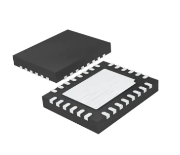
Açıklama: RF güç amplifikatörünün ön gerilimini ayarlamak için aktif ön gerilim kontrol cihazı. Besleme ve sıcaklık dalgalanmaları karşısında ön gerilimi sabit tutmak üzere düzenlenmiş drenaj gerilimi ve aktif ön gerilim akımı kontrolü sağlar.
Anahtar Özellikler: Tek besleme gerilimi 5 V ila 16,5 V, ayarlanabilir drenaj gerilimi 3–15 V, ~500 mA’ya kadar ayarlanabilir drenaj akımı, QFN paketi.
Teknik Özellikler
Parça Numarası Tanımı
HMC920 is an integrated active bias controller designed for Class-A RF and microwave amplifiers. LP5E stands for 32-lead 5mm × 5mm exposed pad QFN surface-mount package. The device is supplied in tape-and-reel lead-free packaging for automated large-volume SMT assembly production.
Temel Elektriksel Performans Parametreleri
This monolithic bias management IC delivers fully regulated drain voltage and dynamically tunes the gate voltage of external amplifiers to maintain fixed quiescent drain current across varying operating conditions. It supports biasing for both enhancement-mode and depletion-mode RF amplifiers working under Class-A operation.
The device runs from a single positive supply voltage ranging from 5 V to 16.5 V. Regulated drain output voltage is adjustable between 3 V and 15 V, while maximum configurable drain bias current reaches 500 mA. An internal negative voltage generator is embedded to supply the negative gate bias required by depletion-mode semiconductor devices.
The closed-loop active regulation architecture stabilizes bias current against supply fluctuations, wide temperature swings, semiconductor process deviations and long-term component aging, eliminating periodic calibration work and preventing RF performance degradation. Built-in protection functions include short-circuit protection with power foldback characteristic, programmable over-current and under-current alarm thresholds, and undervoltage lockout alarm for the main input supply.
Automated power-up and power-down sequencing ensures safe amplifier startup and shutdown. A dedicated enable pin controls the activation state of the bias loop, and a trigger output pin enables daisy-chained sequential power management for multi-stage amplifier systems. Typical quiescent supply current is 20 mA under standby mode and 35 mA during normal operation. The internal low-noise LDO minimizes power supply noise injection into RF signal paths for cleaner spectral performance.
Ambalajlama ve Montaj Teknik Özellikleri
The component is encapsulated in a compact 32-pin exposed thermal pad QFN plastic package with 5mm × 5mm body dimensions. The bottom exposed pad enhances thermal dissipation efficiency and improves grounding integrity for high-frequency RF circuits. Moisture Sensitivity Level is MSL1, meaning no time restriction applies to reflow soldering procedures after vacuum packaging is opened. Continuous tape reel feeding is fully compatible with automatic pick-and-place machinery for uninterrupted mass electronic assembly lines.
Çevre ve Uyum Standartları
The industrial operating temperature range spans -40 °C to +85 °C, supporting reliable long-term operation in wireless communication infrastructure, microwave transceivers, aerospace equipment and precision measurement instruments under harsh ambient conditions. Manufactured with lead-free production processes, the IC complies with RoHS3 and REACH global environmental directives. The highly integrated single-chip design replaces dozens of discrete passive and active bias components, simplifies RF amplifier power circuit layout and shortens hardware development cycles for microwave systems.
Tipik Uygulama Alanları
Cellular communication base station RF front-end amplifier bias circuits
Wireless broadband infrastructure and microwave radio transceiver modules
VSAT satellite communication ground terminal equipment
Aerospace and military ruggedized RF microwave systems
Precision RF signal generators and laboratory test & measurement instruments


