






| МОДЕЛЬ П/Н | СЕРИИ | КОЛИЧЕСТВО ЛАБОРАТОРИЙ/КЛБ | УРОВЕНЬ СКОРОСТИ | КОЛИЧЕСТВО ЛОГИЧЕСКИХ ЭЛЕМЕНТОВ / ЯЧЕЕК | ВСЕГО БИТОВ ОЗУ | КОЛИЧЕСТВО ВХОДОВ/ВЫХОДОВ | НАПРЯЖЕНИЕ - ПИТАНИЕ | ТИП КРЕПЛЕНИЯ | РАБОЧАЯ ТЕМПЕРАТУРА | УПАКОВКА / КЕЙС | УПАКОВКА УСТРОЙСТВА ПОСТАВЩИКА |
|---|---|---|---|---|---|---|---|---|---|---|---|
| XC7Z030-2FFG676C | Zynq-7000 SoC | 9.825,00 | -2,00 | 125,000 | 9768960 | 228 | ~1.0 V | Крепление на поверхность | 0 °C ~ +85 °C | FCBGA-676 | 676-FCBGA (27×27 мм) |
XC7Z030-2FFG676C
Производитель: Xilinx
Логические ячейки: ~27,600
Встроенная оперативная память (eRAM): ~1,0 Мб
Количество входов/выходов: ~676 контактов
Упаковка: FFG?676
Рабочая температура: Коммерческий (от 0°C до +85°C)
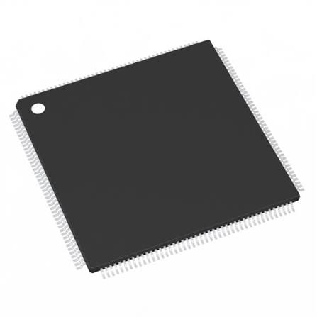
Технические характеристики
Part Number Interpretation
This is a heterogeneous all-programmable SoC from Xilinx Zynq-7000 family, fabricated on 28nm process technology. It combines dual-core ARM Cortex-A9 processor subsystem and mid-capacity Artix-7 programmable logic, designed for cost-sensitive commercial embedded control, low-to-medium speed signal processing and entry-level vision applications.
- XC7Z030: Mid-range mainstream device in Zynq-7000 series
- -2: Speed Grade 2, standard performance grade with sufficient timing margin for general high-frequency logic design
- FFG676: 676-ball flip-chip FCBGA package
- C: Commercial temperature range, junction temperature: 0°C ~ +85°C
On-Chip Hardware Architecture
1. Processing System (PS)
- Dual-core ARM Cortex-A9 processor, maximum frequency up to 1GHz
- Each core equipped with 32KB instruction cache and 32KB data cache; 512KB shared L2 cache
- Integrated NEON SIMD floating-point unit for multimedia decoding and basic digital signal acceleration
- Peripherals: Dual Gigabit Ethernet, USB 2.0 OTG, SD/MMC, CAN, UART, SPI, I2C, general GPIO
- Secure boot function available to protect system firmware
2. Programmable Logic (PL, Artix-7 architecture)
- Total Logic Cells: 125440
- DSP48E1 arithmetic units: 480 pieces, applied for small-scale FFT, digital filtering, single-channel image processing and simple matrix computation
- Total Block RAM: 9.1Mb
- Multiple MMCM and PLL modules to generate various clock signals and suppress jitter
- No integrated high-speed serial transceivers
3. I/O and Monitoring Module
- Usable user I/O pins: 360
- I/O bank voltage configurable from 1.2V to 3.3V, supporting LVCMOS, LVDS and common differential signal standards
- Dual-channel 12-bit XADC on chip: Real-time monitoring of chip temperature, internal power voltages and external analog signals
Power Characteristics
Nominal core voltage: 1.0V
Independent power domains for PS and PL parts
Typical total power consumption: 7W ~ 22W. A small heatsink is required for continuous full-load operation.
Packaging & SMT Requirements
- Package: 676-ball FCBGA
- Moisture Sensitivity Level: MSL3. Reflow soldering must be completed within 168 hours once vacuum packaging is opened
- Lead-free design, fully compliant with RoHS regulations
- Supplied in anti-static trays for mass PCB production
Environmental Reliability
Only suitable for constant-temperature indoor commercial and laboratory environments, not applicable to outdoor industrial scenarios with extreme temperature fluctuations.
It supports bitstream encryption and SEU error detection, featuring stable operation for indoor automation equipment, consumer vision devices and desktop measuring instruments.
Main Application Scenarios
- Medium-precision industrial motion controllers, main control units for small automated machinery
- Single-camera embedded visual inspection equipment, industrial image acquisition terminals
- Multi-channel conventional data loggers, environmental monitoring instruments
- Main control boards for small indoor medical devices
- Front-end processing units for miniature video surveillance
- Low-cost embedded SOM modules and lightweight algorithm verification platforms


