






Технические характеристики
This is a high-performance dual-link LVDS serializer developed by THine Electronics, designed to convert massive parallel RGB TTL video signals into differential LVDS serial signals, mainly driving high-frame-rate 1080P and QXGA resolution display panels to simplify wiring and suppress electromagnetic interference.
Определение номера детали
THC63LVD1023B is the official model of the multi-bit dual-channel LVDS transmitting chip series, featuring enhanced asynchronous dual-channel transmission and multiple data mapping modes compared with conventional single-link LVDS devices.
Core Function and Electrical Parameters
The chip supports input dot clock frequency ranging from 10MHz to 160MHz, converting up to 67-bit parallel CMOS/TTL image data into two groups of 5-channel differential LVDS output signals. Each differential channel reaches a maximum transmission rate of 1.12Gbps, with total data throughput up to 5.6Gbps. It flexibly switches among four working modes: single TTL input single LVDS output, single TTL input dual LVDS output, dual asynchronous TTL input dual LVDS output and port signal distribution mode. The built-in PLL phase-locked loop circuit requires no external crystal oscillator and matching components. Users can configure clock edge sampling via hardware pins, and double-edge data sampling is available to improve data transmission efficiency. Three sets of standard LVDS data mapping protocols are embedded to match mainstream display panel specifications. Reduced swing LVDS output can be enabled to lower electromagnetic radiation during high-speed operation, and a built-in pseudo-random signal generator facilitates factory production testing and signal troubleshooting. The device adopts single 3.3V power supply design, with independent power-down control pin to enter ultra-low power standby mode when the screen is shut down, reducing idle power consumption effectively. Input logic level is compatible with 3.3V LVTTL standard, which can be directly connected to main control chips such as FPGA and ARM.
Технические требования к упаковке и сборке
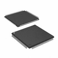
Standard packaging is 144-pin LQFP surface mount package with overall dimension 20mm×20mm. It belongs to MSL3 moisture sensitive component, and reflow soldering construction must be completed within 168 hours after opening the original vacuum packaging. Tray and tape-and-reel packaging are both provided to adapt to automated SMT placement and mass production assembly on production lines.
Экологические стандарты и стандарты соблюдения нормативных требований
Normal operating temperature range is -20℃ to +70℃, and industrial temperature version can work stably from -40℃ to +85℃. The whole product adopts lead-free manufacturing process and complies with universal environmental protection and restriction standards. Differential signal transmission greatly cuts the quantity of connecting wires between mainboard and screen, optimizes PCB wiring difficulty and improves long-distance signal transmission stability.
Типичные области применения
High refresh rate LCD TV mainboard screen drive circuit and professional desktop high-resolution monitor signal conversion board Industrial high-definition human-machine touch display and embedded equipment large-size TFT screen interface conversion module Vehicle central control large screen, full LCD instrument panel and rear seat entertainment display signal transmission unit Medical imaging display equipment, precision testing instrument display terminal and long-distance video signal extension equipment Digital signage advertising machine, multi-screen splicing sending card and industrial equipment centralized display drive board
LXB Semicon supplies original THine THC63LVD1023B dual-link high-speed LVDS transmitter integrated circuit


