






| 모델 P/N | 시리즈 | 실험실/CLBS 수 | 속도 등급 | 논리 요소/셀 수 | 총 램 비트 | I/O 수 | 전압 - 공급 | 마운팅 유형 | 작동 온도 | 패키지 / 케이스 | 공급업체 디바이스 패키지 |
|---|---|---|---|---|---|---|---|---|---|---|---|
| XCZU3EG-3SFVC784E | Zynq® UltraScale+™ MPSoC(EG) | 8,82 | -3,00 | ~154K 로직 셀 | ~7.6Mbit | 0 | 0.85 V | 표면 실장(FCBGA) | 0°C - 100°C(TJ) | FCBGA-784 | 784-FCBGA |
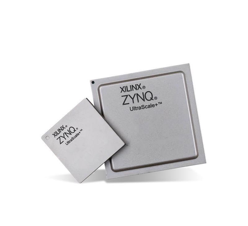
사양
부품 번호 분석
This is AMD Xilinx Zynq UltraScale+ MPSoC without integrated RF converters, built on 16nm FinFET process for low-power embedded computing, vision and industrial control.
- XCZU3EG: Entry-level low-power member of Zynq UltraScale+ MPSoC family
- -3: Speed Grade 3, optimized for low power consumption with moderate timing performance
- SFVC784: 784-ball flip-chip FCBGA package
- E: Extended industrial temperature grade, junction temperature range: -40°C ~ +125°C
Complete On-Chip Hardware Architecture
1. Processing System (PS: ARM Subsystem)
- Quad-core ARM Cortex-A53 application processors
- Dual-core Cortex-R5F real-time cores for safety-critical and low-latency control tasks
- Integrated Mali-400 MP2 GPU for lightweight graphical rendering
- Built-in hardware video codec supporting multi-channel video encoding and decoding
- Abundant peripherals: Gigabit Ethernet, USB 3.0, SD/eMMC, CAN, UART, SPI, I2C, GPIO
- On-chip hardware security unit for secure boot, AES encryption and IP anti-tampering protection
2. Programmable Logic Fabric (PL: FPGA Domain)
- Total Logic Cells: 154,000
- DSP48E2 arithmetic blocks: 720 units for filtering, FFT, sensor data calculation and image algorithm acceleration
- Total Block RAM + UltraRAM: 9.2 Mb
- Multiple MMCM and PLL clock management tiles to support multi-clock domain design and jitter reduction
- Configurable I/O banks compatible with LVCMOS, LVDS and mainstream differential signal standards
3. High-Speed Serial Transceivers
8 GTY high-speed serial lanes, maximum per-lane rate up to 16.375 Gbps. Supports PCIe Gen3, Aurora and high-speed inter-board data transmission protocols.
전원 공급 장치 사양
Independent power domains are assigned to PS, PL and transceivers. Typical core logic voltage is 0.85 V. Dynamic voltage and frequency scaling is available to cut power consumption under light load.
Typical overall power consumption ranges from 6 W to 20 W, passive heat sinks are applicable for compact embedded devices.
Packaging & SMT Assembly Specifications
- Package: 784-pin flip-chip FCBGA ball grid array
- Moisture Sensitivity Level: MSL3; reflow soldering must be completed within 168 hours after vacuum packaging is opened
- Lead-free construction, fully RoHS compliant
- Supplied in anti-static trays for automated industrial PCB mass production
Environmental and Reliability Characteristics
Supports ultra-wide extended temperature range, stable operation under extreme temperature and strong electromagnetic interference conditions.
Equipped with SEU radiation error correction, partial dynamic reconfiguration and redundant real-time core functions, ideal for automotive electronics, outdoor industrial equipment and aerospace lightweight embedded terminals requiring high reliability.
일반적인 애플리케이션 시나리오
- Industrial controllers, servo drive main control units and factory edge gateways
- Embedded machine vision systems, industrial camera image acquisition and defect detection terminals
- Automotive domain controllers, vehicle-mounted display and advanced driver assistance peripheral modules
- Portable data recorders, vibration monitoring instruments and miniature precision measurement equipment
- Intelligent surveillance edge computing nodes and IoT multi-sensor convergence terminals
- Medical portable diagnostic equipment front-end control and signal processing boards


